

A fundamental objective of materials engineering is the control of the micro/nanostructure, which largely governs the mechanical properties of materials. But despite substantial progress, our ability to simultaneously tune a broad range of microstructural parameters, in both bulk and thin film materials, is still limited.
We have developed a new methodology based on magnetron sputtering to synthesize thin films with exceptional microstructural control via systematic, in situ seeding of nanocrystals into amorphous precursor films. When the amorphous films are subsequently crystallized by thermal annealing, the nanocrystals serve as preferential grain nucleation sites and determine their micro/nanostructure. We have used this methodology to precisely tailor the size, geometry and spatial distribution of nanostructured grains in structural (TiAl) as well as functional (TiNi) thin films. We have also elucidated and contrasted the crystallization mechanisms in seeded and unseeded amorphous films using in situ TEM annealing experiments.
This synthesis methodology is likely to be applicable to a broad class of amorphously grown materials (semiconductors, ceramics, etc.) and also other types of physical vapor deposition processes like evaporation.
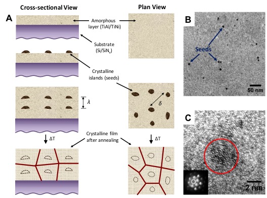
(A) First, an amorphous layer of the thin film material is deposited on the substrate. Next, crystalline nanoscale domains (seeds) are deposited on the amorphous layer. A second amorphous layer is then deposited to sandwich the seeds. These steps are repeated until the desired film thickness is obtained. Following the deposition, the film is thermally annealed to crystallize it. The seeds serve as grain preferential nucleation sites during annealing and hence the grain heights and diameters scale with λ and δ, respectively. (B) TEM bright-field image showing a dispersion of crystalline Ti seeds on an amorphous TiAl layer. (C) HR-TEM image showing the atoms on the (0001) plane of a Ti seed (red circle) surrounded by the amorphous TiAl matrix. The CBED pattern of the seed is shown in the inset.
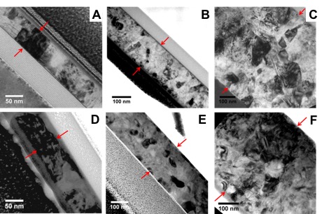
Examples of films synthesized with the new methodology. (A, D) TiAl and TiNi films with a single grain across the thickness. (B, E) TiAl and TiNi films with multiple grains across the thickness. (C, F) TiAl and TiNi films with a gradient microstructure.