

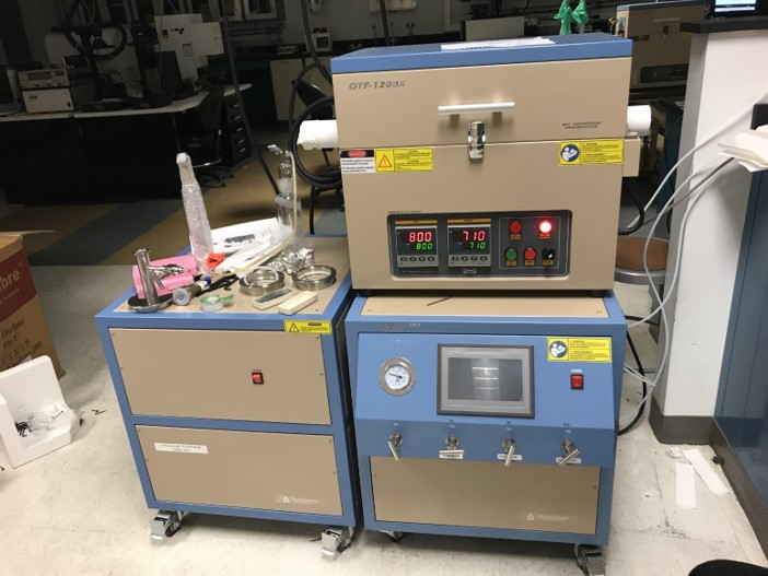
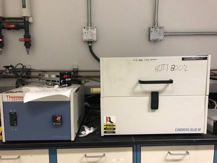
Material Synthesis
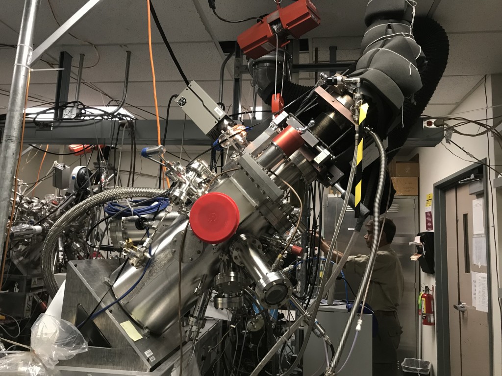
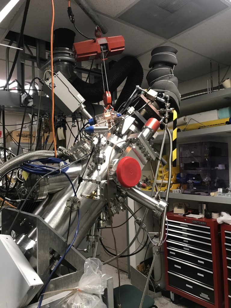
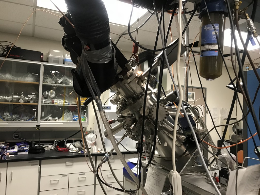
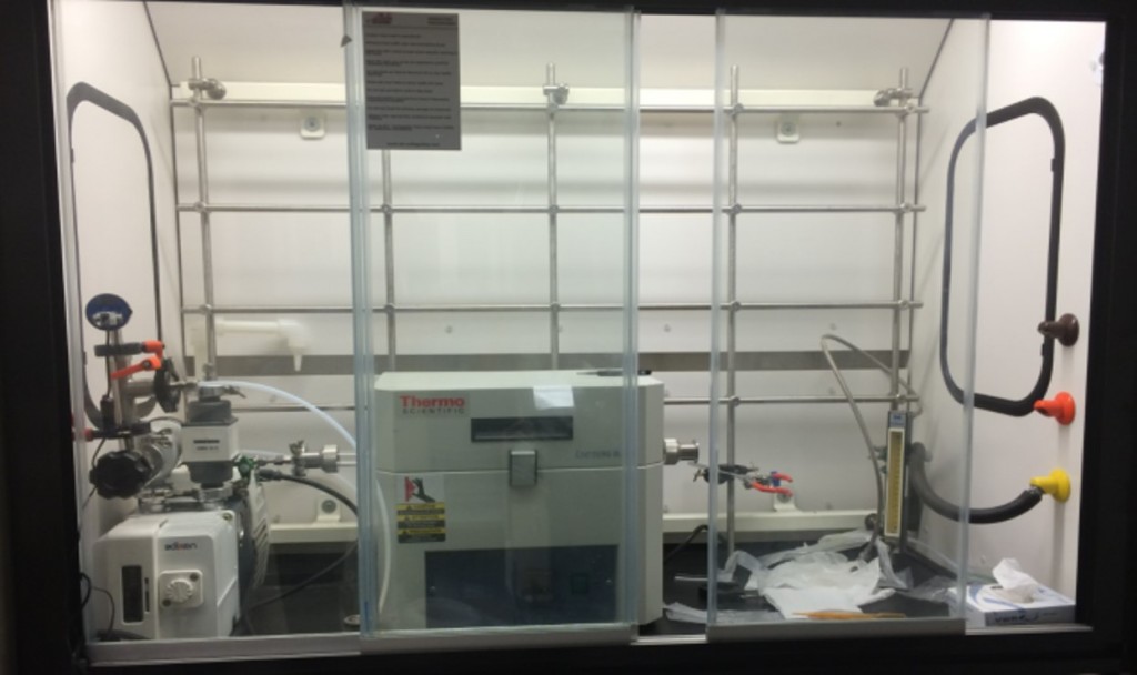
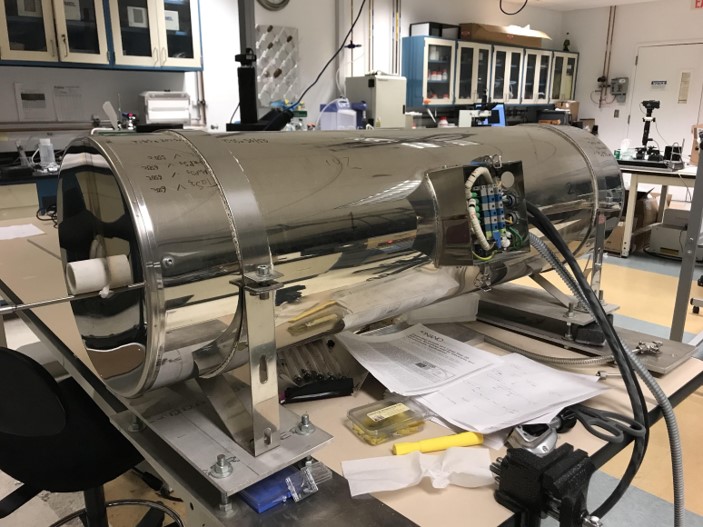
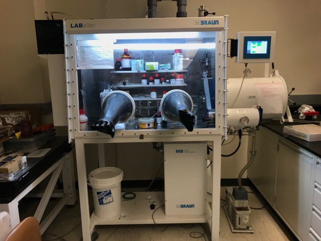
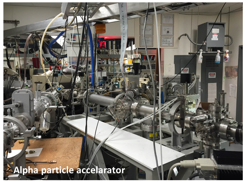
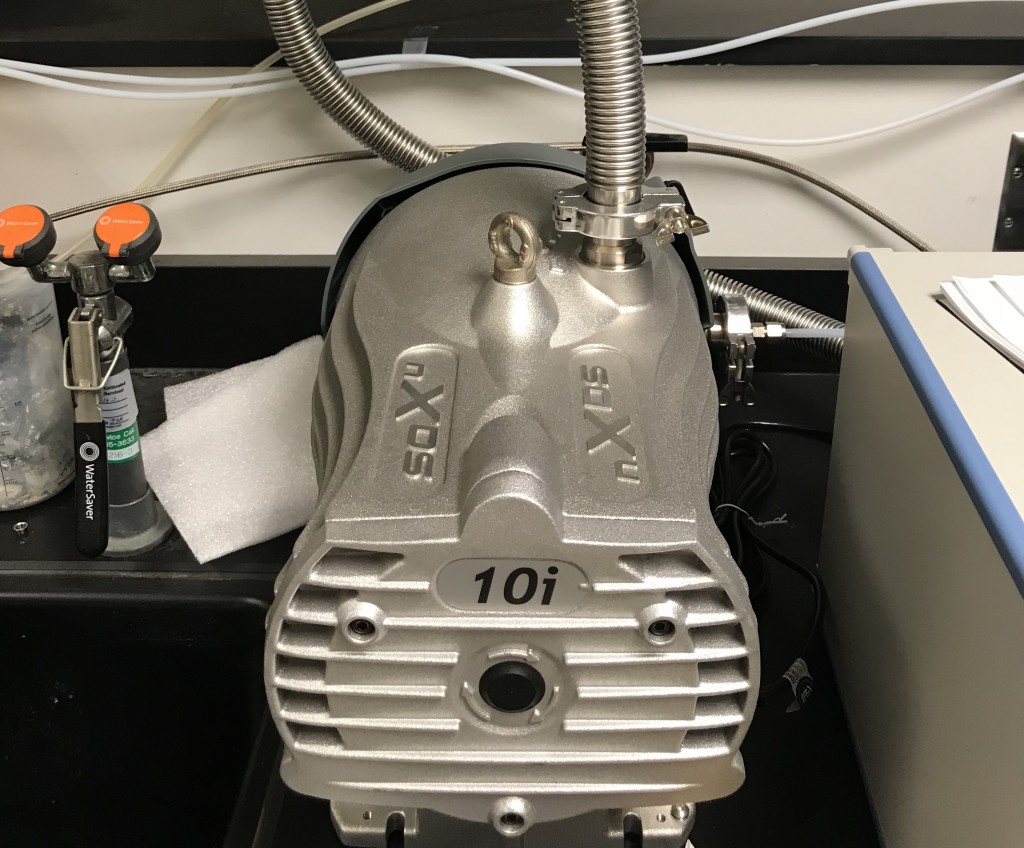
Our material synthesis capabilities cover rather broad range of techniques. Examples include; molecular beam epitaxy (MBE), chemical vapor deposition (CVD), physical vapor deposition (PVD), hydrothermal synthesis, polymer growht (2D polymers), and bulk crystal growth.
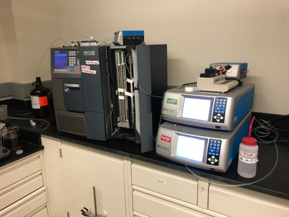

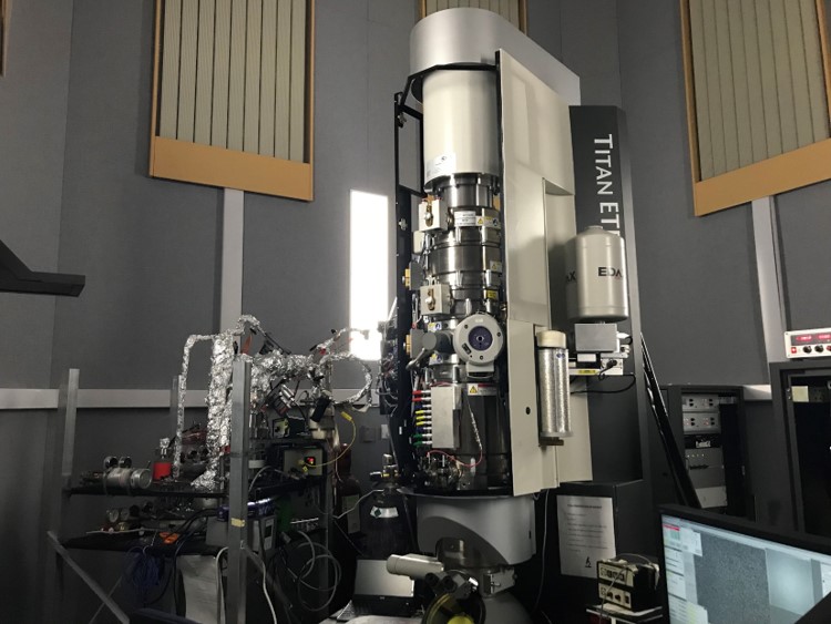
Material Characterization: Spectroscopy, microscopy, and electronic transport
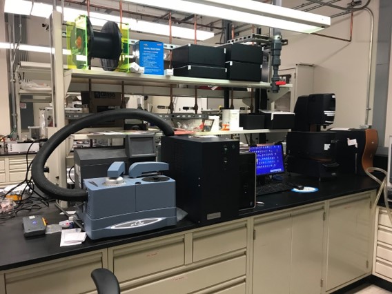
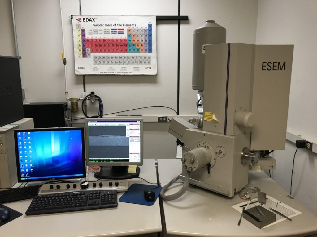
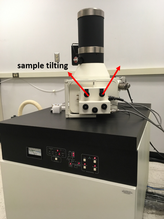
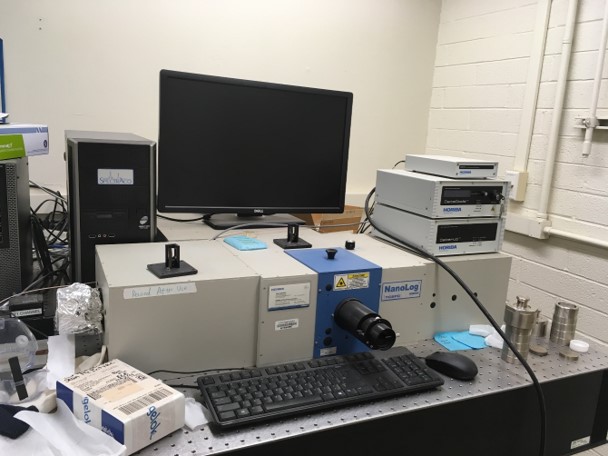
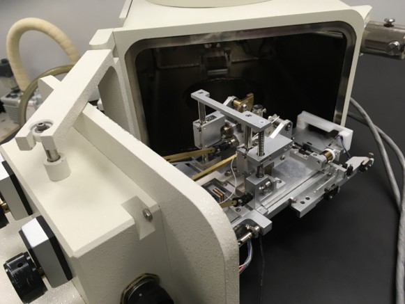
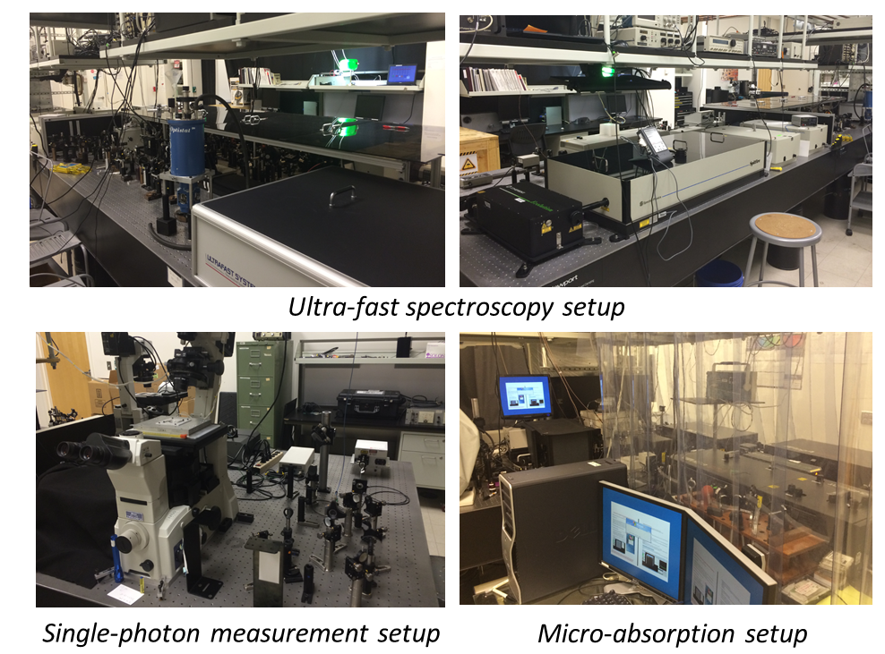
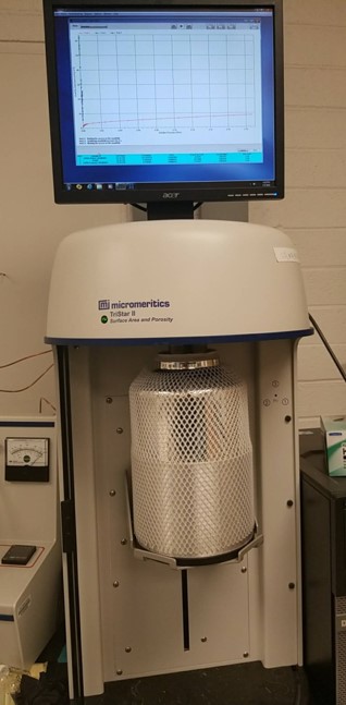
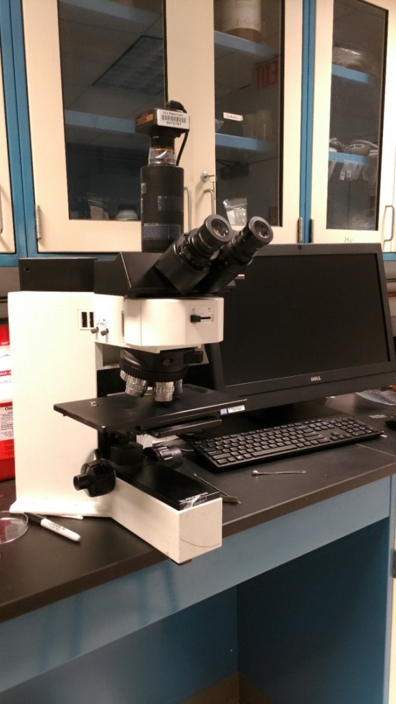
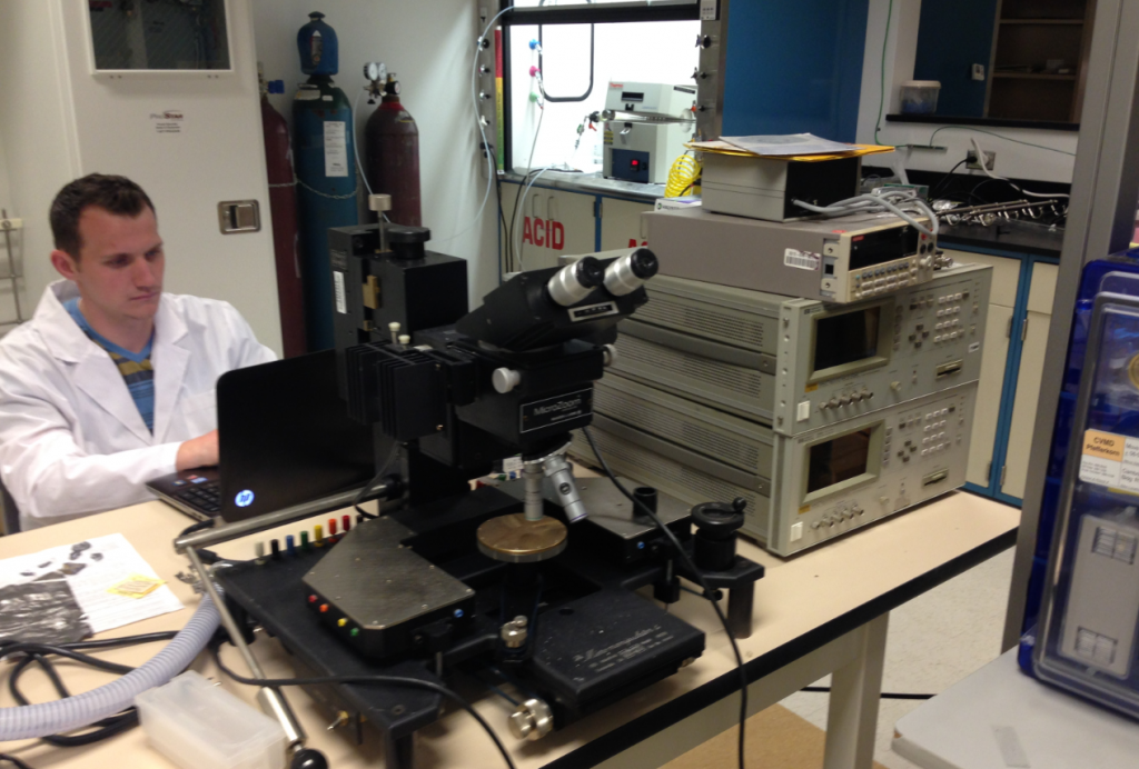
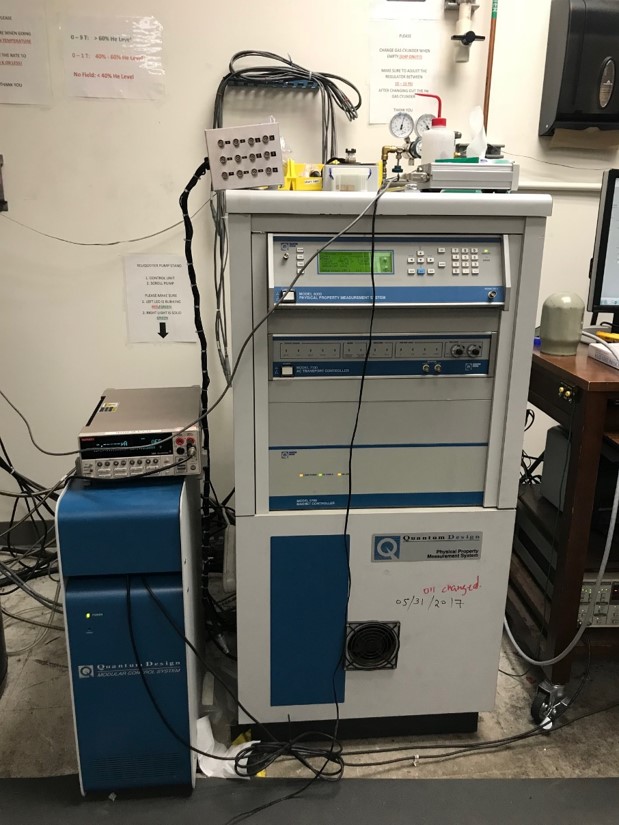
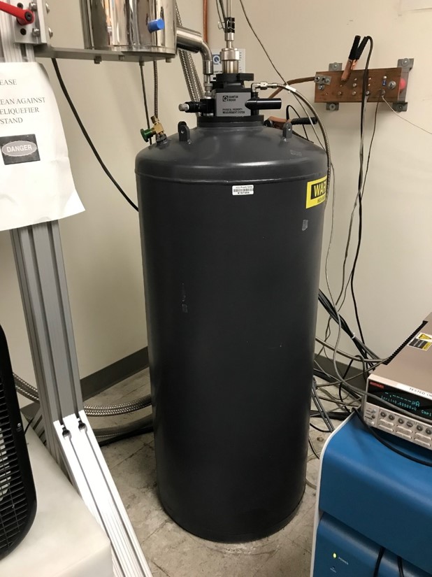
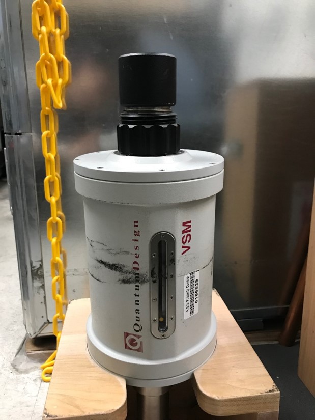
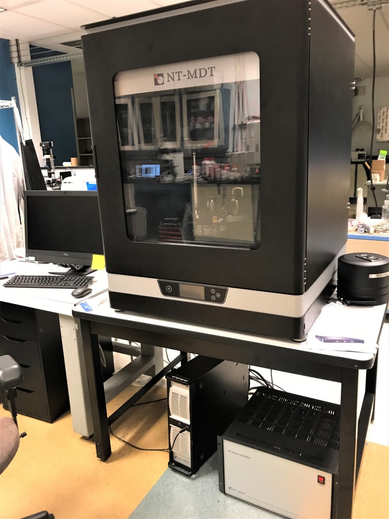
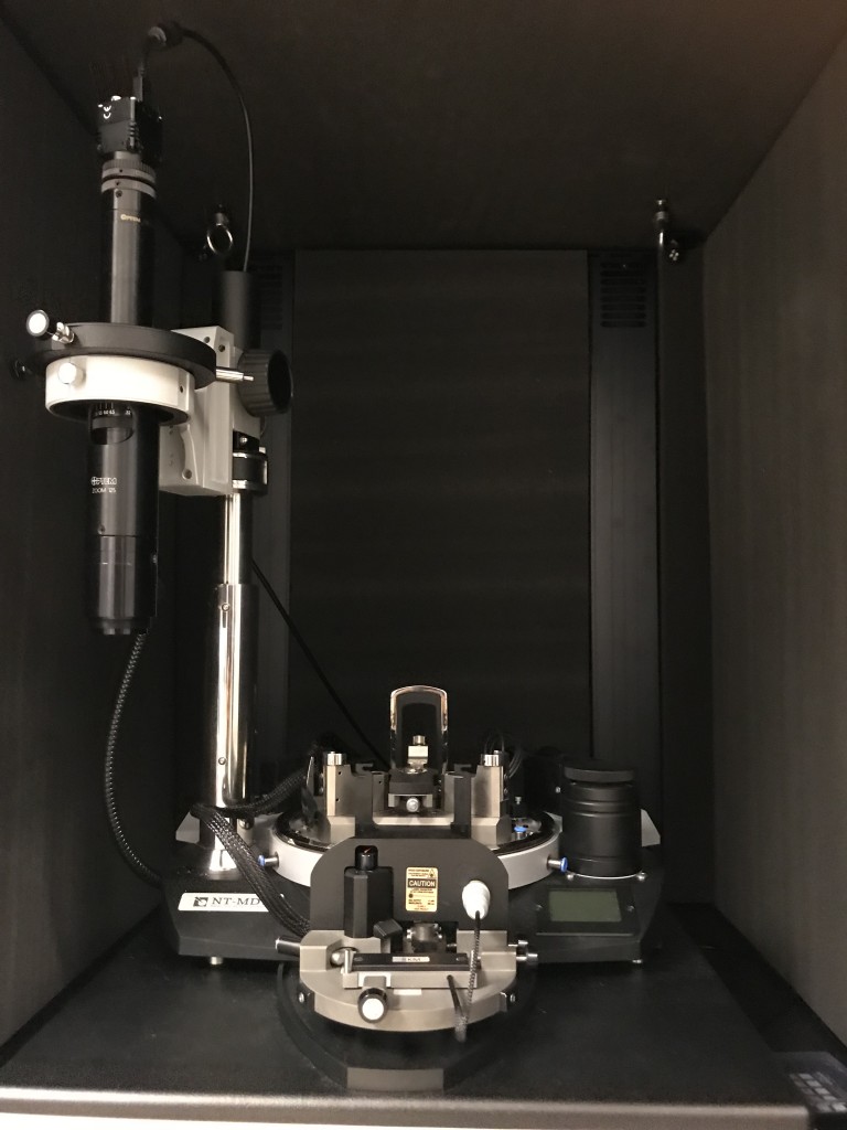
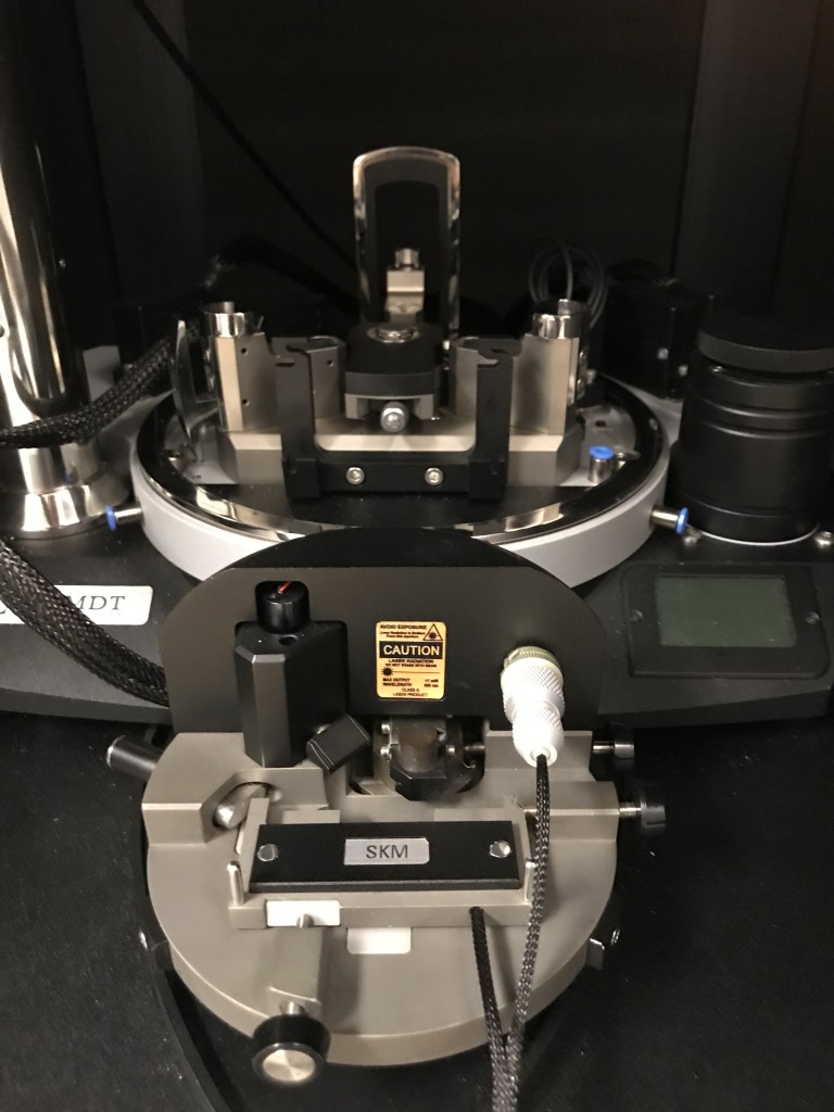
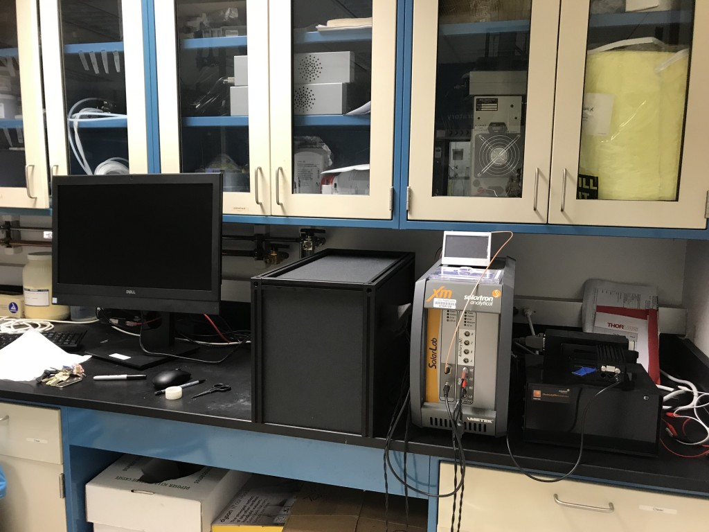
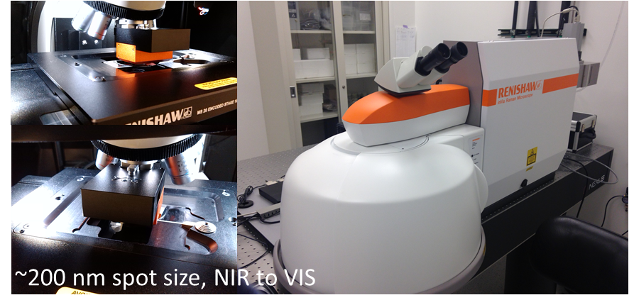
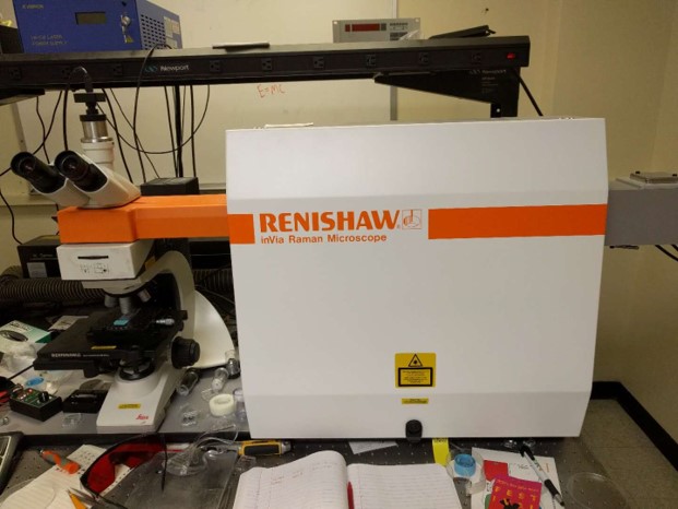
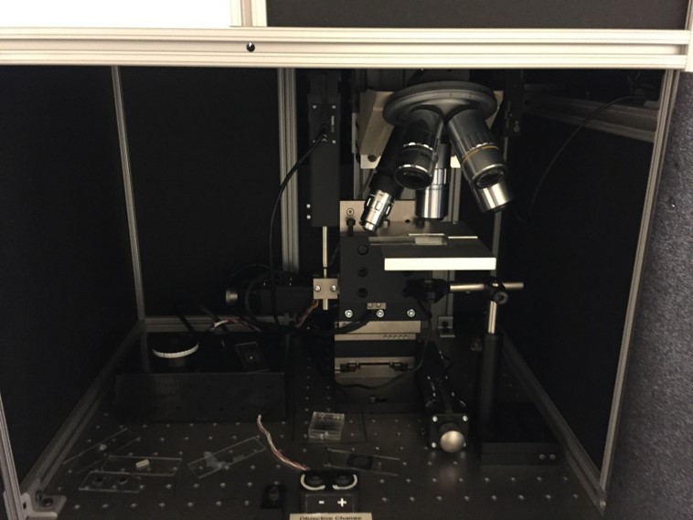
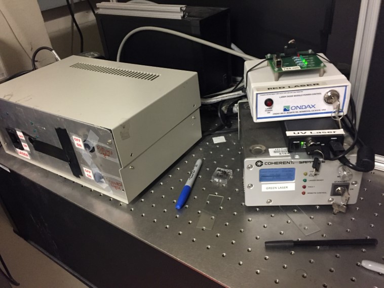
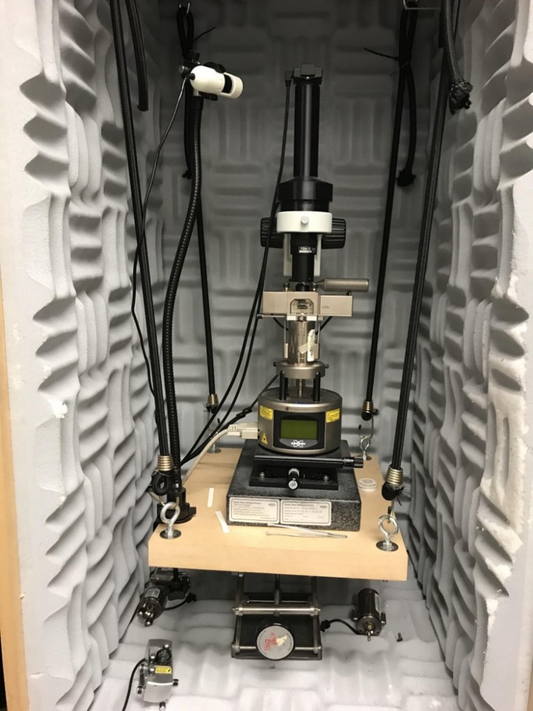
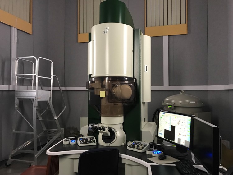
The team specializes in material characterization of nanomaterials. Our techniques include but not limited to; atomic force microscopy (AFM), scanning tunneling spectroscopy (STS), scanning tunnelling spectroscopy (STM), Transmission electron microscopy (TEM and STEM), electronic characterization, optical spectroscopy. Measurement range covers from low 4K to high 1400K. AFM, STM, and STS measurements can be performed under controlled gaseous environment, liquid, and vacuum conditions. PPMS, VSM, MPMS, nanoindentation, and AFM nanoindenter for electronic, magnetic, and mechanical measurements. Catalysis station, nano-catalysis AFM/STM setup for artificial photosynthesis, catalysis, and electrochemistry.
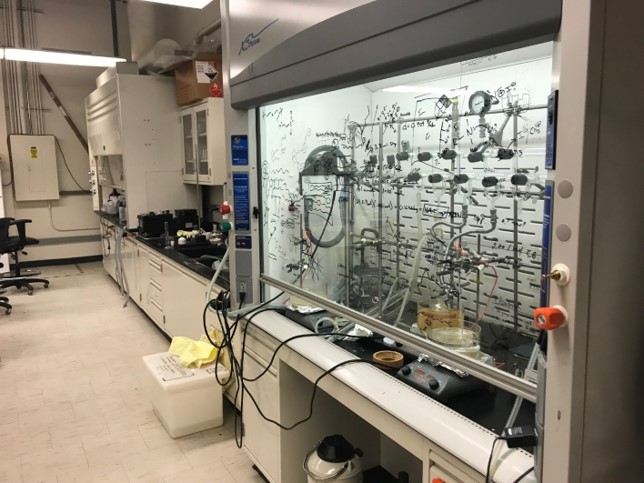
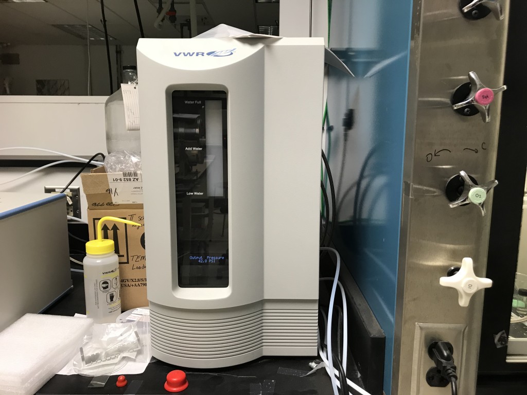
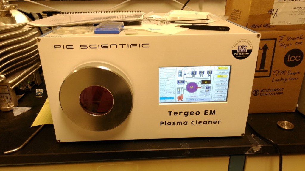
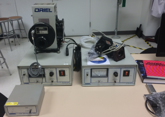
Material processing
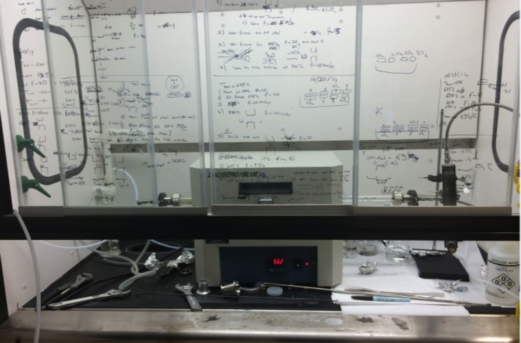
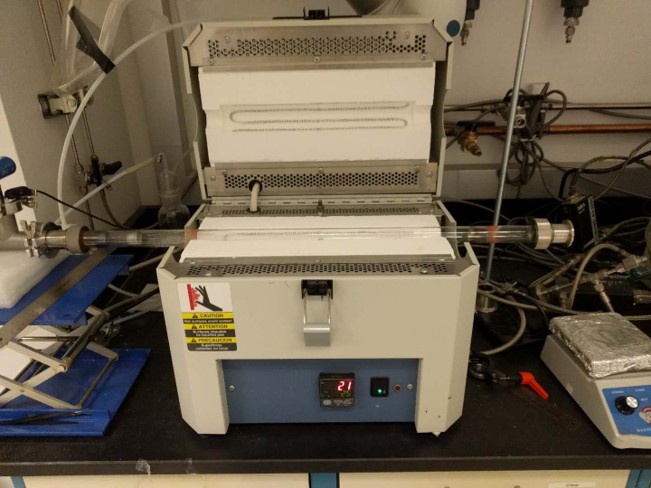
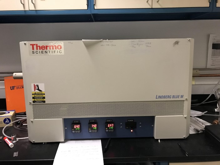
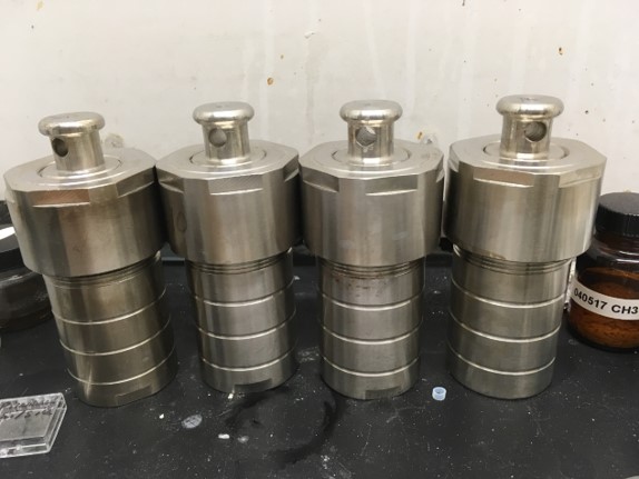
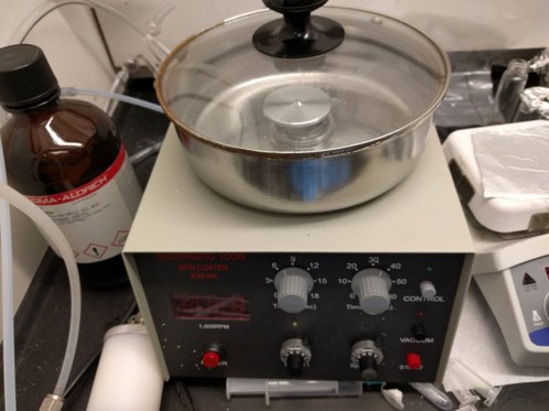
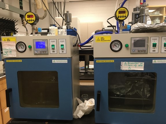
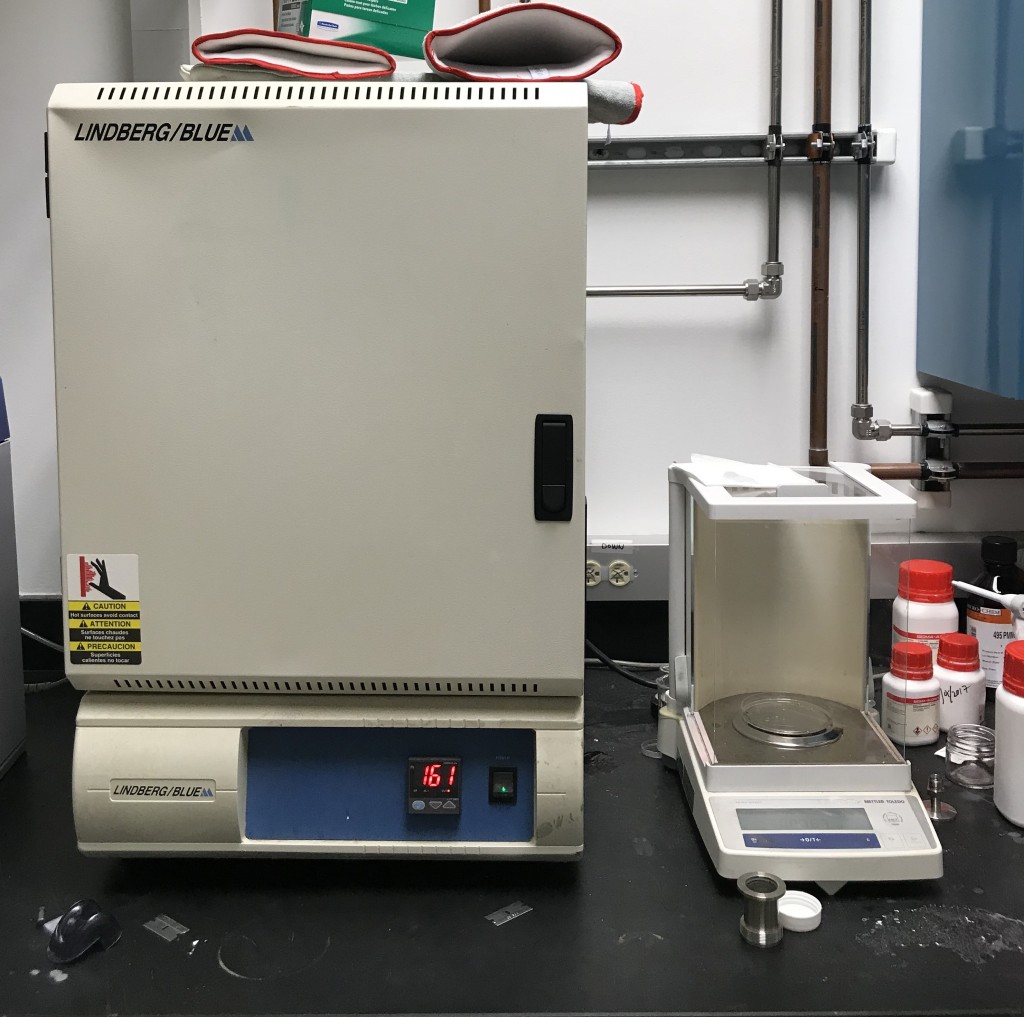
Our laboratory has the following processing techniques available to us; liquid phase exfoliation station, plasma processing chamber, intercalation chemistry bench, vacuum furnaces, spin coaters, solar generators, and mechanical testers
Shared facilities Coming soon