MEMS for in situ Materials Studies
Materials at the micrometer and submicrometer scale exhibit mechanical properties that are substantially different from bulk materials. With the increasing miniaturization of devices, an accurate characterization of micro/nanoscale materials is necessary to ensure their reliability and performance. Precise characterization is also essential for a fundamental understanding of mechanisms that govern size dependent material responses.
We use a MEMS based testing device (developed at Prof. Saif’s lab at UIUC) to study the mechanical behavior of nanoscale thin films through pure uniaxial tension. This device avoids the problems of handling, gripping and aligning of nanoscale samples by co-fabricating the film specimens with the device. The device has built-in gauges that enable the measurement of both stress and strain in the nanoscale films during deformation. More importantly, the small footprint of the device (3mm×10mm×150µm) makes it compatible with SEM and TEM straining holders and allows quantitative in situ SEM and TEM experiments.
We are currently interested in developing MEMS devices for in situ characterization of nanowires (co-fabricated and externally fabricated) at elevated temperatures. We are also interested in developing MEMS platforms for the thermal, mechanical and electrical characterization of nanostructured materials, with the aim of elucidating the role of microstructural heterogeneity in determining these properties.
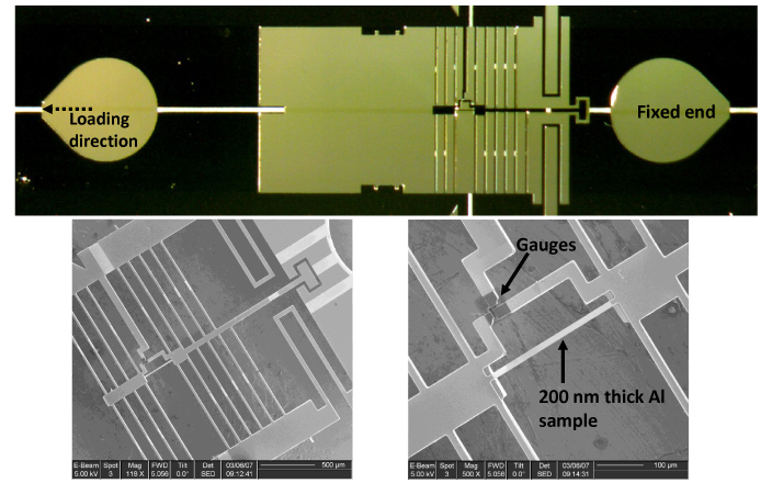
Top : Optical image of the MEMS device for testing of nanoscale thin film samples. Higher magnification SEM micrographs of the device and the sample are shown below.
Related Publications
1. W. Kang, J. Rajagopalan and M. T. A. Saif, “In situ uniaxial mechanical testing of small scale materials – a review,” Nanoscience and Nanotechnology Letters 2, 282-287, 2010 (pdf)
2. J. Han, J. Rajagopalan, and M. T. A. Saif, “MEMS-Based testing stage to study electrical and mechanical properties of nanocrystalline metal films,” Proceedings of SPIE, Vol. 6464, 64640C , 2007 (pdf)