


With the growing interest in 2D semiconductors in both academia and industry, a natural progression will be in understanding how these materials can be doped for electronic applications. While doping transition metal dichalcogenides (TMDs) is in no way a new feat, controllable doping and scalable synthesis of doped samples have thus far been insurmountable challenges in this area of interest. Furthermore, studies on doped TMDs are almost exclusively focused on degenerately doped samples, with dopant concentrations below 1 at. % rarely being reported in the literature.
Three methods are being investigated in parallel to explore the possibilities for doping TMDs (MoS2, MoSe2, WS2, WSe2) and other 2D semiconductors with both n-type and p-type dopants. Our team is seeking to answer the following questions:
- What are the upper and lower limits of dopant concentrations achievable with each technique?
- Can dopants be homogeneously distributed with each technique?
- How tightly can dopant concentrations be controlled using each technique?
Our team is exploring three different directions to answer these fundamental questions;
Chemical Vapor Deposition
Chemical vapor deposition (CVD) is a non-equilibrium technique for growing thin films of materials. CVD relies on transporting precursors to a substrate at high temperature, at which point they will adsorb to the surface and react together, forming the desired material. The process is very sensitive to the surface energy of the substrate being grown on, making CVD very suitable for growing single layers of material. Furthermore, large-scale synthesis has been realized for a variety of processes using CVD, with full coverage of two-inch wafers having been demonstrated using this technique.
By introducing an additional precursor during synthesis which contains a desired dopant, our team is looking to introduce both n-type and p-type dopants into various monolayer TMD films.
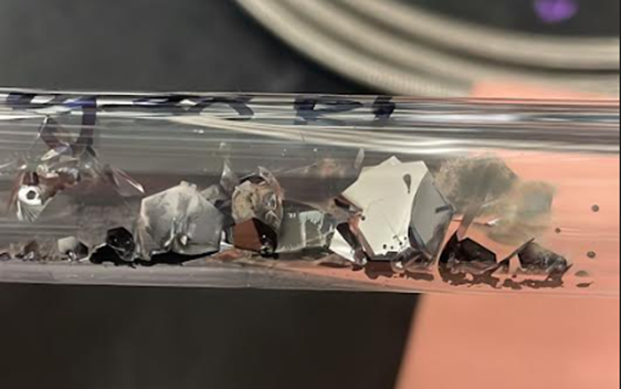
Crystal growth
Chemical vapor transport (CVT) is a process for growing high-purity bulk crystals. CVT works by sealing precursor compounds into a quartz ampoule under a moderate vacuum, then subjecting the precursors to a temperature gradient. The precursors react and condense as crystals at the colder zone of the ampoule. Crystals with lateral dimensions of several centimeters have been previously grown by our team using this technique. In principle, CVT can be used to incorporate highly controlled amounts of dopants into 2D semiconductors by precisely controlling the amount of dopant precursor used in the reaction.
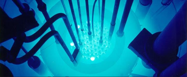
Neutron Transmutation Doping
Neutron transmutation doping (NTD) is a relatively new and somewhat unconventional technique for introducing dopants into materials. In NTD, samples are placed near the core of a nuclear reactor, where they are bombarded by thermal neutrons released from the core during fission processes. Neutron transmutation refers to a process by which an atomic nucleus captures one of these thermal neutrons. Capturing a neutron will transform the atom into a heavier isotope of the same element. Depending on the identity of this new isotope, it will then decay, typically by beta decay. This causes an atom of one greater atomic number than the original atom that captured the thermal neutron to be substituted into the lattice.
Materials being explored currently are WSe2, WS2, InSe, and In2Se3. These crystals were chosen for a variety of reasons, the most important of which is that the primary decay products (rhenium for tungsten-based crystals and tin for indium-based crystals) are known to be electronically active n-type dopants in their respective structures.