

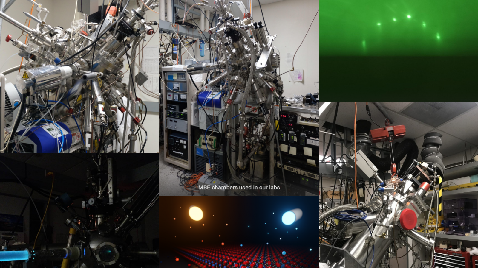
Molecular beam epitaxy
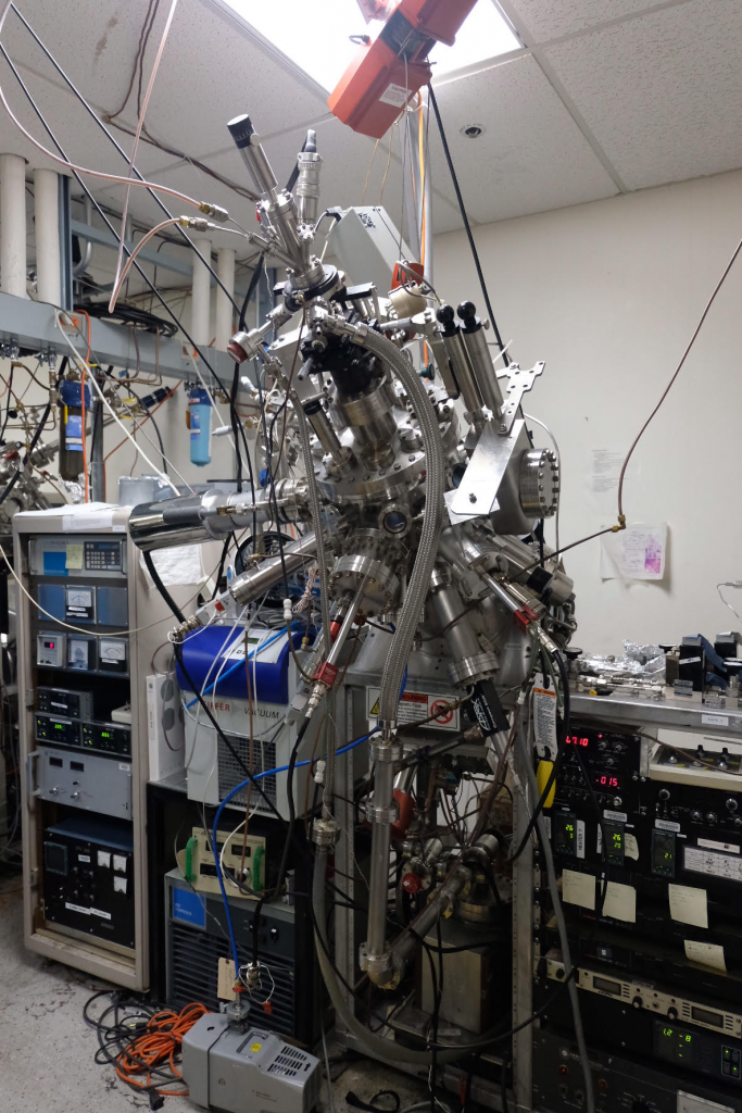
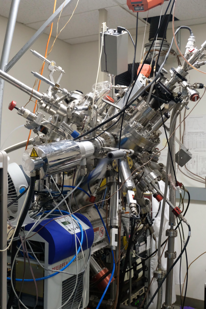
Molecular beam epitaxy (MBE) is an epitaxy method for thin or two-dimensional (2D) film deposition of highly crystalline materials. MBE is considered as one of the cleanest growth method since it is operated under ultra-high vacuum. MBE setup consists of Knudsen effusion cells (K-cells) or electron beam evaporators that heat up ultra pure elements. The elemental precursors are evaporated by these evaporators and impinge on a heated substrate. The flux rate, composition and doping level of the films are precisely controlled by changing the evaporator temperature, which is important for 2D materials synthesis. Our MBE system equipped with reflection high-energy electron diffraction (RHEED) for in-situ characterization of the deposited films. The electron beam from the RHEED gun is diffracted by the atoms at the surface and the diffraction pattern is imaged on the fluorescent screen. The pattern shows the crystallinity of the films and the growth mode of the epitaxy. The intensity oscillation of the diffraction pattern determines the growth rate.
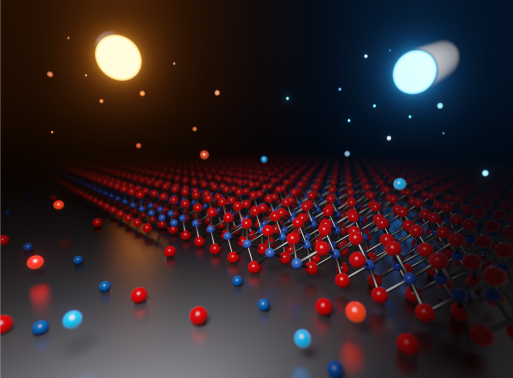
Our team mainly focuses on the discovery of new 2D quantum materials by MBE synthesis technique. Some of the target materials include 2D MnTe and MnSe magnets, Janus MnSeTe layers for skyrmionics, transition metal dichalcogenides for excitonics and charge density wave materials. While synthesizing these materials, our team aims to answer the following fundamental questions using MBE growth technique.
- How can we synthesize high quality defect and grain boundary free quantum materials in 2D form using MBE?
- How can we introduce technologically relevant point defects into quantum materials?
- How can one stabilize new phases of matter by controlling the substrate temperature, substrate type, or interface characteristics?
Pulsed Laser Deposition
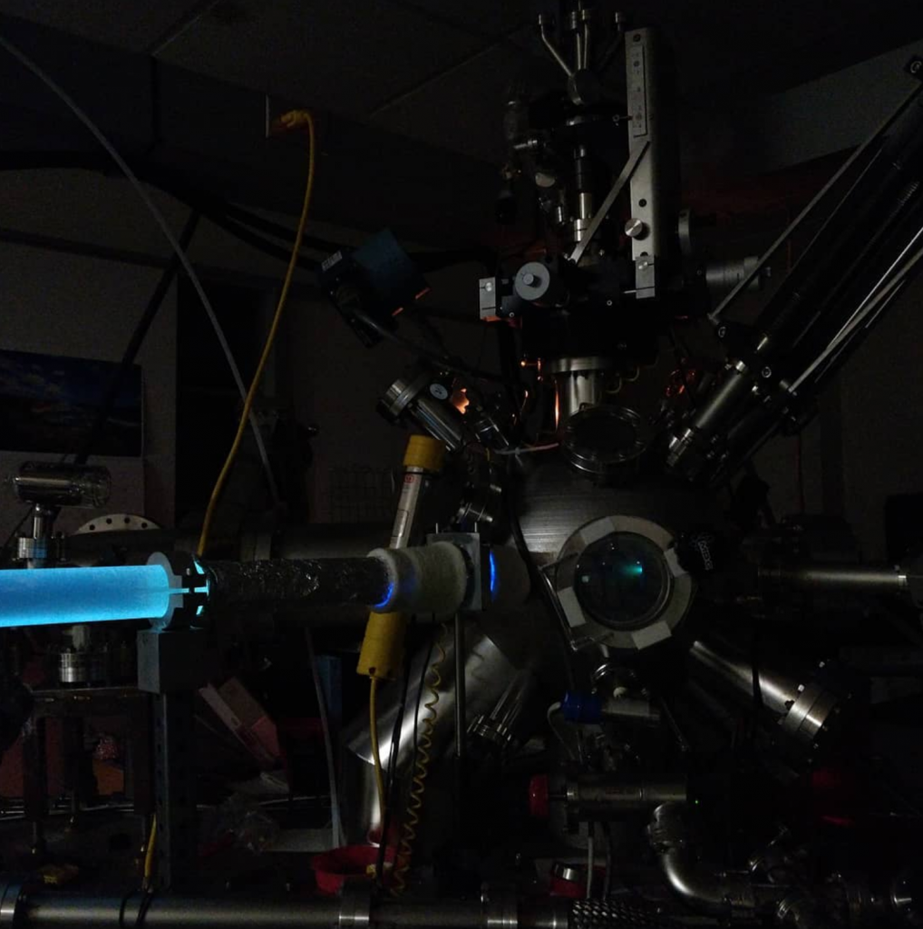
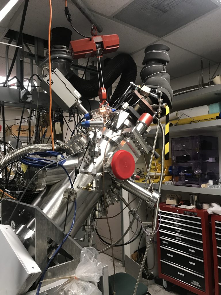
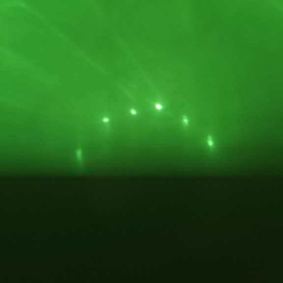
Another common method used in our laboratory for epitaxial synthesis of pulsed laser deposition (PLD). In this technique, we employ highly energetic laser operating at 1ps to ns time duration. Our high-power pulsed laser beam is focused inside a vacuum chamber to strike a target of the material that is to be deposited. This material is vaporized from the target (in a plasma plume see in the figure below) which deposits it as a thin film on a substrate (such as a silicon wafer facing the target). This process can occur in ultra high vacuum or in the presence of a background gas, such as oxygen which is commonly used when depositing oxides to fully oxygenate the deposited films.
Typical materials of interest include h-BN (boron nitride) as 2D dielectrics, YBCO superconducting films, BSCCO superconductors, and any other semiconducting materials. Some of the fundamental questions include;
- How can we employ pulsed laser deposition technique in synthesizing 2D quantum materials?
- Can we discover new quantum materials and new phases when growth process is highly non-equilibrium?
- How can we engineer defect density in quantum materials during PLD growth?
Select publications
Our team has produced a large number of Nature, science, and other high impact journals on these topics over the years and since 2014 at Arizona State University. Full list can be access at Google Scholar profile.