Research
Research Interests:
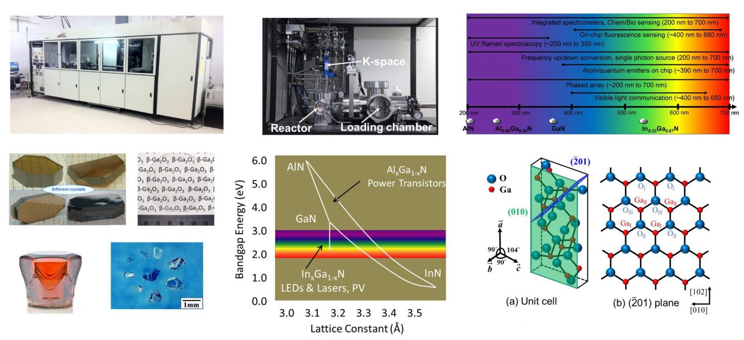
Broad research interests span the fields of solid-state electronics, optoelectronics and photonics, semiconductors, device physics, and nanotechnology. Specific interests include third-generation wide/ultrawide bandgap (WBG/UWBG) semiconductors (GaN and nitride alloys, Ga2O3, AlN, BN, and diamond) for applications in electronics (e.g., power electronics and ICs, WBG/UWBG CMOS and RRAM for computing, RF/microwave devices and MMICs, sensors) and photonics (e.g., optoelectronic devices, waveguides, nonlinear optics, quantum photonics), MOCVD epitaxial growth, nanofabrication and nano-scale characterization, new physics, materials, and devices for future solid-state (opto)electronics and photonics.
Research Details:
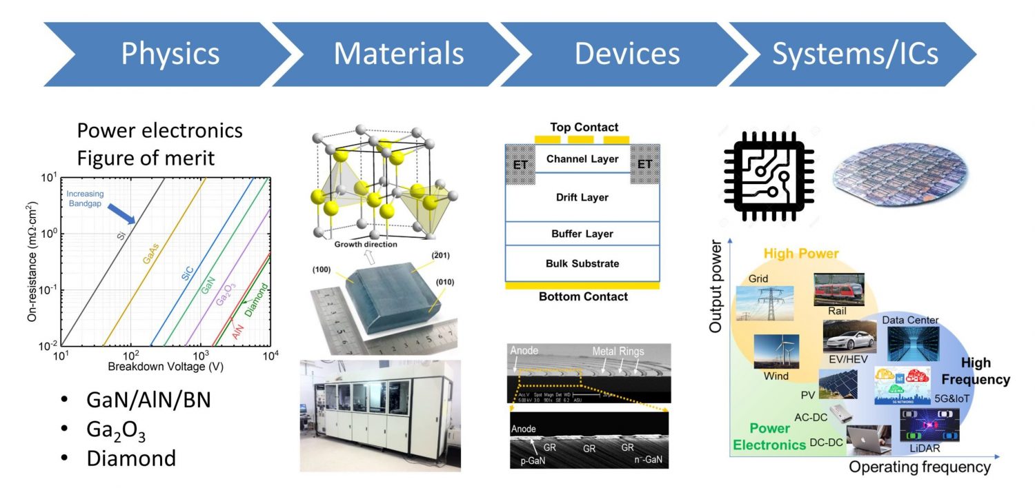
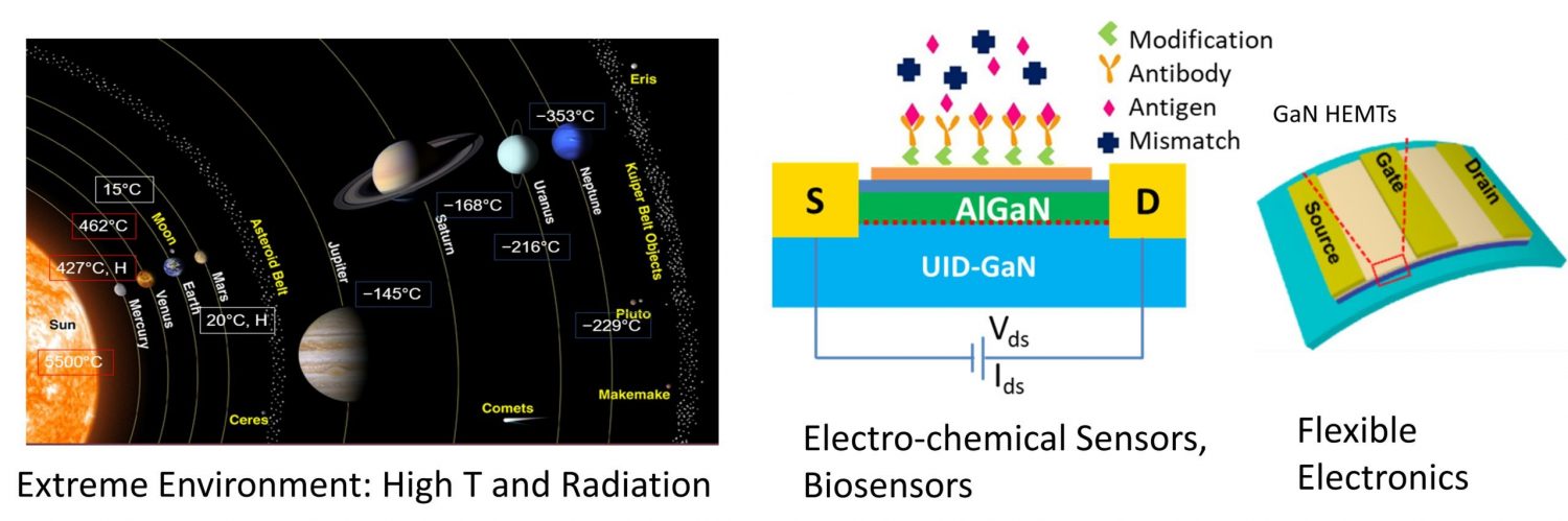
The research at the Semiconductor Materials and Devices Group is focused on the development of novel and advanced solid-state devices and systems for power electronics, energy efficiency, renewable energies, next-generation communication systems, extreme-environment applications (e.g., high temperature and radiation), UV-visible integrated photonics, and biochemical sensing applications. Our research involves MOCVE/MBE epitaxial growth, nanofabrication, and characterization of electronic and optical semiconductor materials, devices, and systems.
Our research can be categorized into the following Thrust Areas:
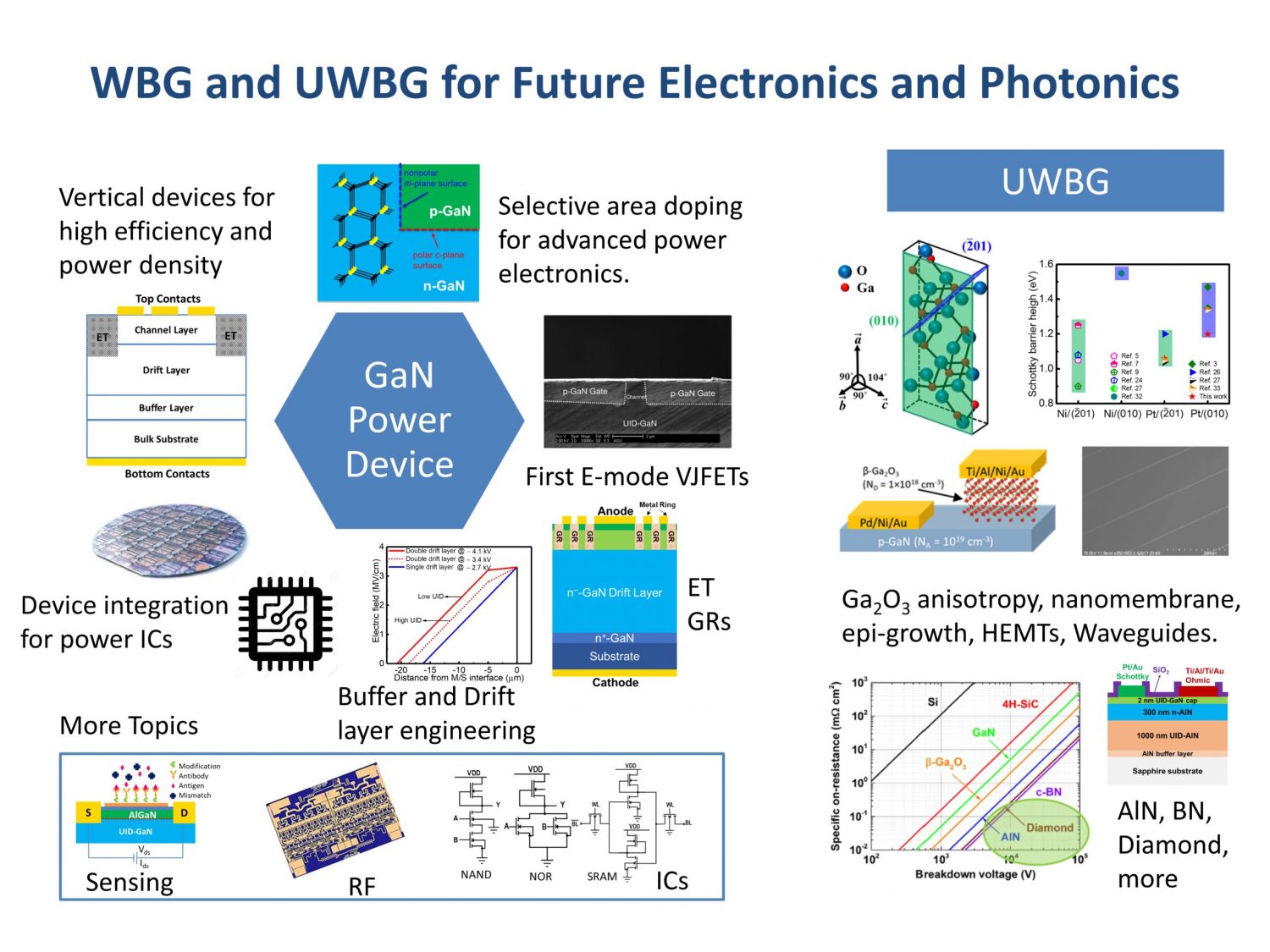
Thrust Area 1: Next-Generation Power Electronics and Computing based on WBG/UWBG Semiconductors.
Thrust Area 2: Extreme-Environment Electronics (e.g., High Temperature and Radiation) and Sensors (e.g., Biochemical).
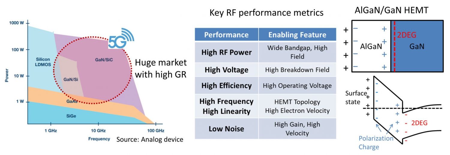
Thrust Area 3: High-Frequency and High-Power RF/Microwaves Electronics and ICs.
Thrust Area 4: MOCVD/MBE Epitaxial Growth, Fundamental Physics and Electronic and Optical Properties of Novel Materials.