Welcome to Compound Semiconductor Device Lab
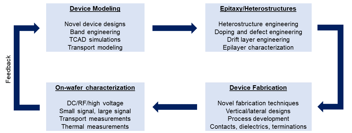
Compound Semiconductor Device Lab at Arizona State University focusses on a vertically integrated approach that closely ties epitaxial growth, heterostructure integration, semiconductor physics, novel device design and nanofabrication techniques for developing next generation high performance electronic devices. We are particularly interested in ultra-wide band gap (UWBG) semiconductors such Ga2O3, III-Nitrides and diamond. These materials exhibit exceptionally high breakdown field strength, which enables the development of electronic devices that are smaller, faster, and more energy efficient. These semiconductors are expected to play a pivotal role in various applications, including electric vehicles, efficient renewable energy transmission, beyond 5G wireless communication, and artificial intelligence.
Vertically Integrated Semiconductor Device Development
News and Updates
September 2023
- Abishek is awarded the MORE Fellowship for Fall 2023. He will be working on device engineering of Ga2O3 using in-situ Ga etching for his Masters thesis. Congrats Abishek.
- David joins our group as an undergraduate research assistant. He will be working on modeling and analysis of diamond based bipolar devices for very high voltage power electronics. Welcome David.
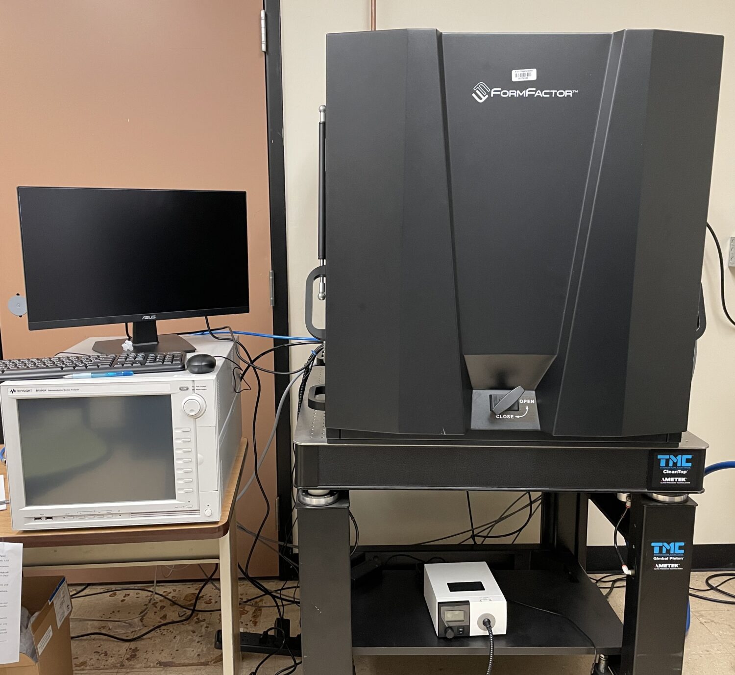
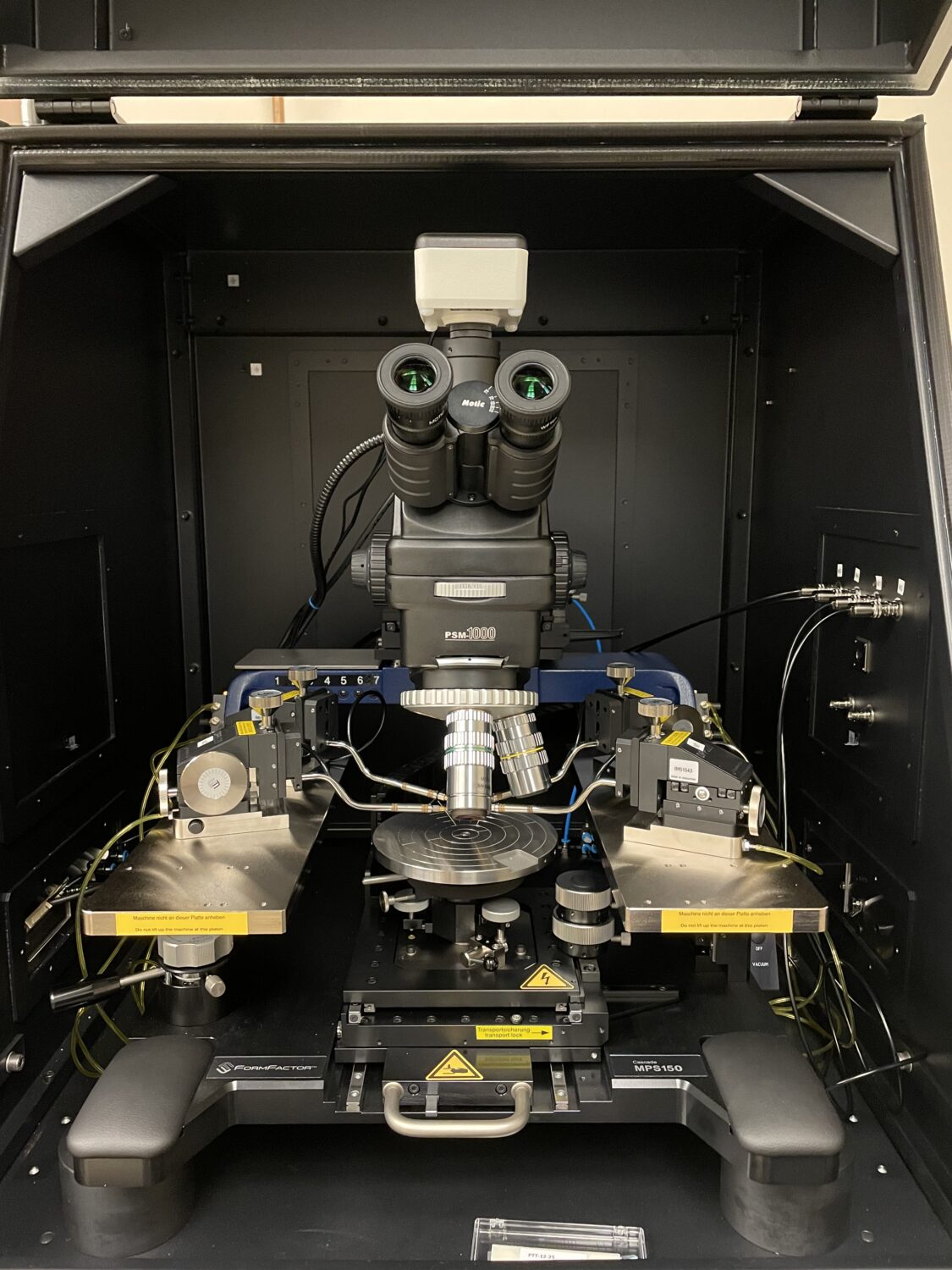
- We add an EPS 150 probe station from Formfactor and a Keysight B1500 semiconductor device analyzer. These instruments will enable high quality DC and pulsed on-wafer characterization of semiconductor devices.
August 2023
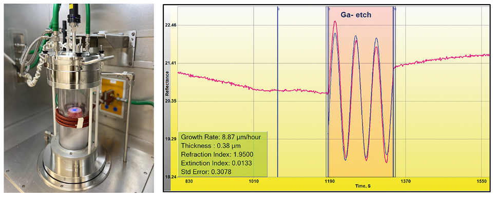
- Our work on Ga etching gets featured in Compound Semiconductor Magazine. In collaboration with Agnitron technologies, we developed a novel in-situ etching method for beta-Gallium Oxide enabling etch rates exceeding 8 microns/hr. Read the full article here.
- Abishek is awarded the TSMC Fellowship for Fall 2023. He will be working on device engineering of Ga2O3 using in-situ Ga etching for his Masters thesis. Congrats Abishek.
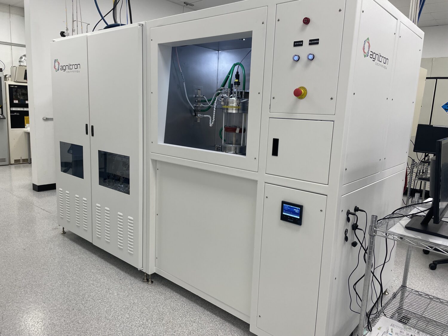
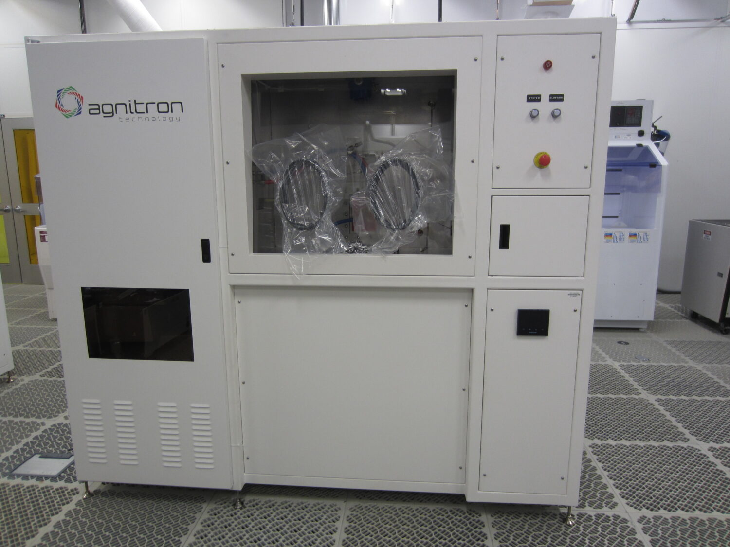
- Our III-Nitride and Oxide MOCVD reactors were delivered to ASU Macro Technology Works. These two reactors will be housed in MTW Solarfab and will be the workhorse for epitaxial growth of UWBG nitride and oxide semiconductors at ASU.
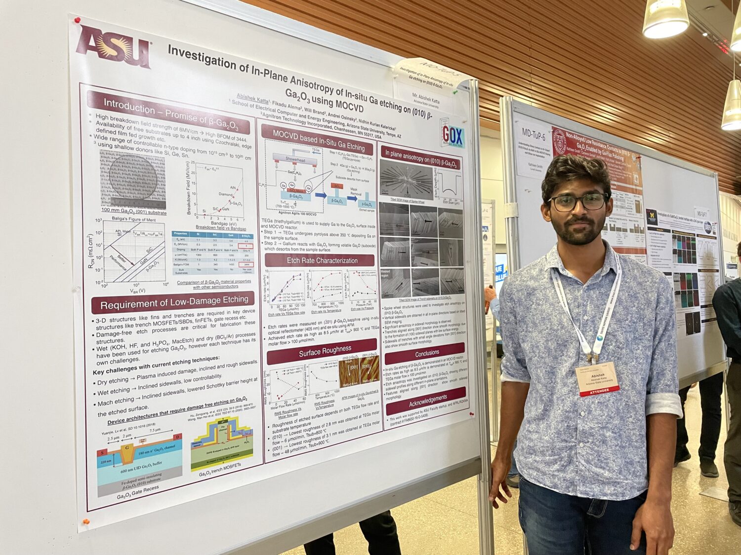
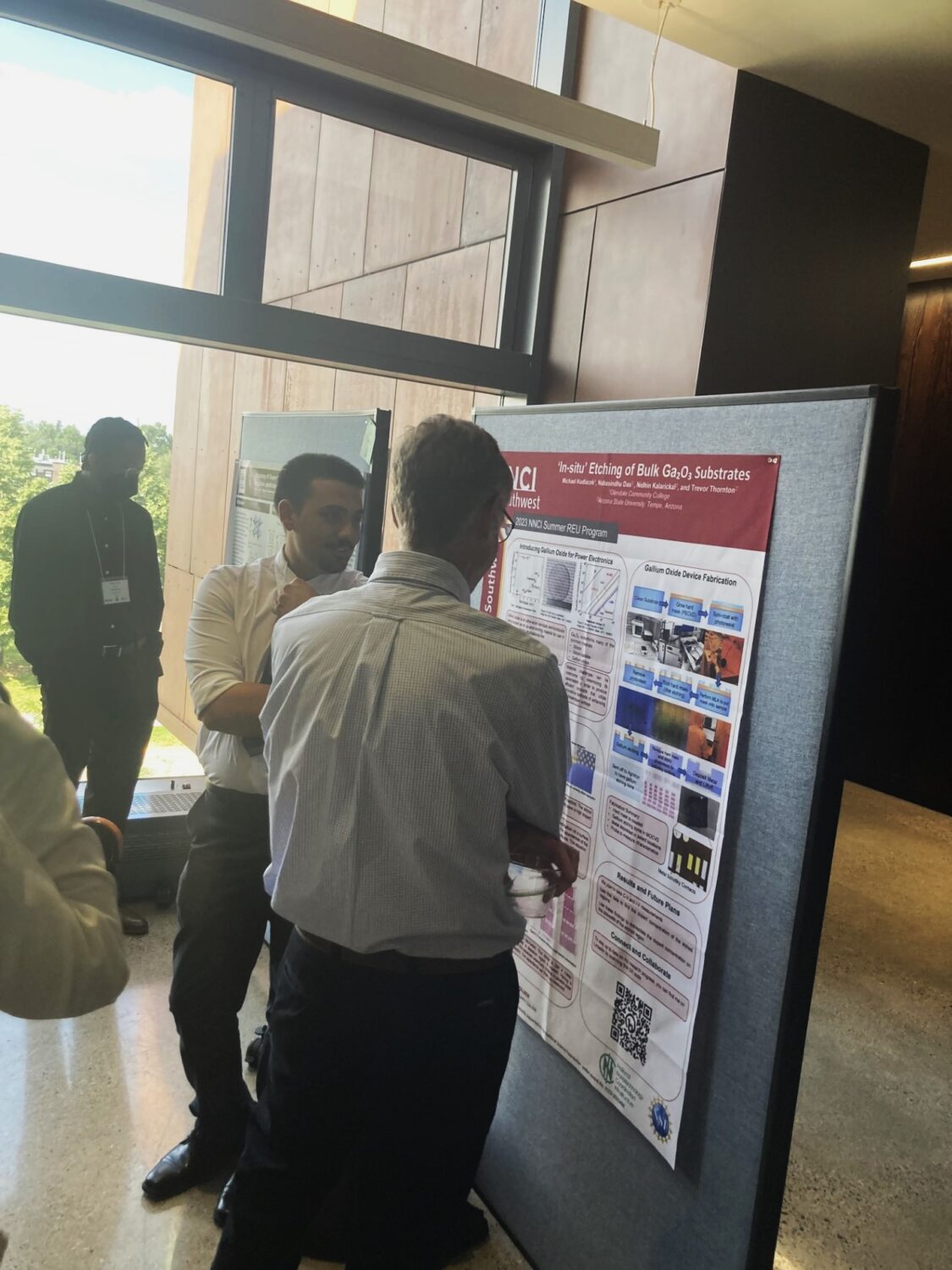
- Abishek gave a poster presentation of his work on ‘Investigation of Etch Anisotropy of MOCVD based in-situ Ga etching on (010) Ga2O3’ at the Gallium Oxide Conference in Buffalo, NY.
July 2023
- Naba gave an oral presentation of his work on ‘Anisotropy of MOCVD based in-situ Ga etching on (010) and (001) Ga2O3’ at the Lester Eastman Conference in Chicago, IL
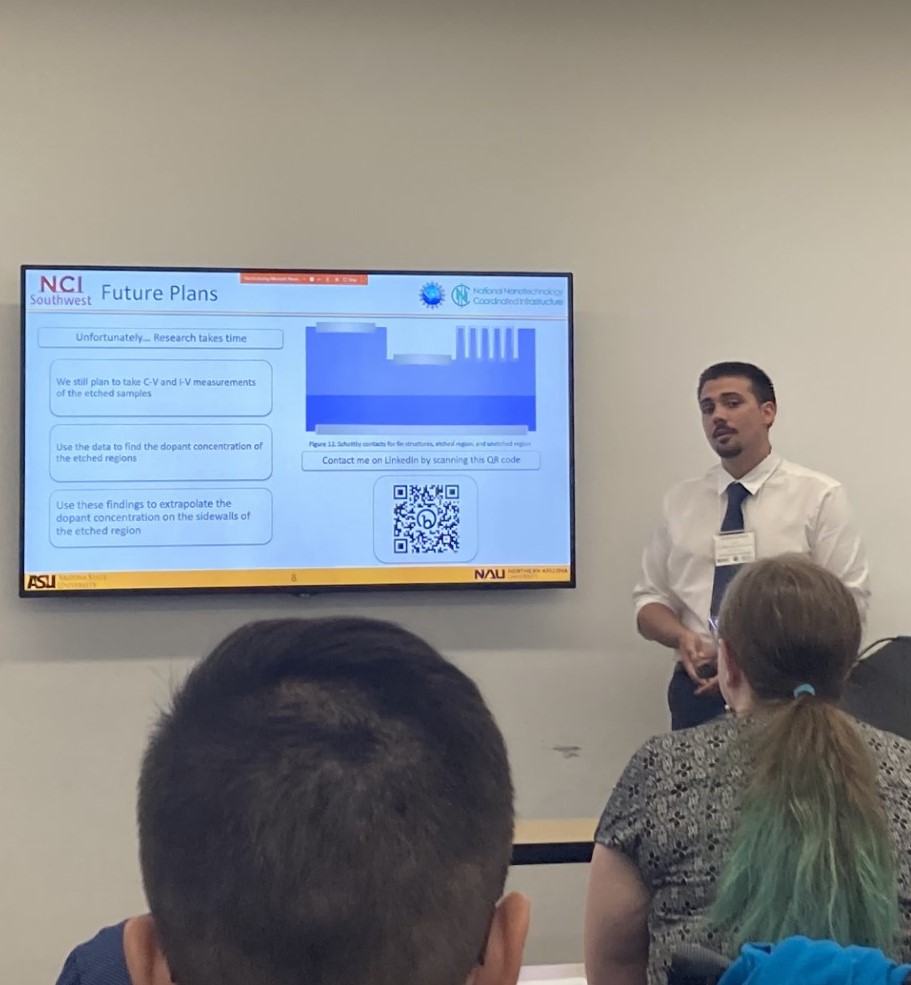
- Michael gave a presentation of his summer research work ‘In-situ etching of bulk Ga2O3 substrates’ at the REU convention in Montana State University.
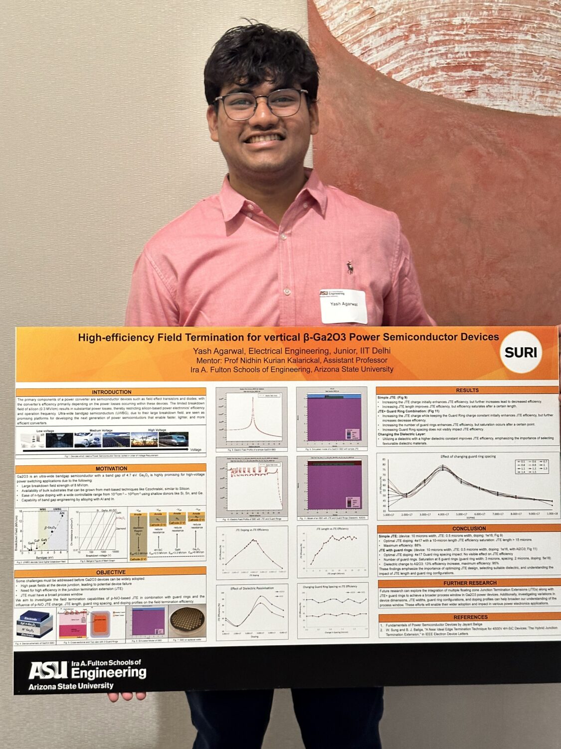
- Yash gave a poster presentation of his work on ‘High efficiency field termination for vertical beta-gallium oxide power semiconductor devices’ at the SURI poster session, 2023.
May 2023
- Our group welcomes Michael Kudlacek. Michael is an NSF REU student from Glendale community college and will be working on novel process engineering for beta-gallium oxide semiconductor technology.
- Our group welcomes Yash Agarwal. Yash is SURI intern from Indian Institute of Technology, Bombay and he will be working on high efficiency field termination for vertical Ga2O3 power devices.
- Nabasindhu Das joins Kalarickal group as a PhD student. He will be working on engineering of lateral Ga2O3 devices for high performance power electronics. Welcome Naba.
January 2023
- Advait Gilankar joins Kalarickal group as a PhD student. He will be working on engineering of vertical Ga2O3 devices for high performance power electronics. Welcome Advait.