Research
Devices for increased power density, speed, and efficiency: Ultra-wide band gap semiconductors (UWBG) like Ga2O3, AlGaN and diamond have the potential to enable unprecedented device performance thanks to the high breakdown field strength making devices smaller, faster, and more efficient. However, this new generation of semiconductors bring with them, a new set of intriguing scientific opportunities and challenges from the materials level to device level. Few examples are,
- Low mobility in UWBG semiconductors- Most ultra-wide band gap semiconductors (Ga2O3, high composition AlGaN etc.) show low room temperature mobility (~100 cm2/V-s), which is an order of magnitude lower than semiconductors like GaN, GaAs etc. Careful device and heterostructure designs are necessary to overcome the low mobility and enable high frequency devices using UWBG semiconductors.
- Breakdown Physics of UWBG semiconductors- Understanding breakdown physics in ultra-wide band gap semiconductors require pushing these semiconductors close to their intrinsic breakdown field (~10 MV/cm). This is extremely challenging as other device components like dielectrics and field terminations breakdown at lower fields. Proper choice and optimization of of dielectrics and field terminations are therefore necessary to achieve near theoretical breakdown performance in these semiconductors.
- Lack of shallow donors/acceptors- Several promising UWBG semiconductors like diamond, AlN etc. only possess deep donors/acceptor levels, meaning that free carrier levels are orders of magnitude lower than substitutional dopant density. This significantly limits transport in these semiconductors resulting in device performance quite far away from the material figures of merit. In addition, the deeper levels can also affect the dynamic performance of electronic devices.
In our work, we try to carefully look at these challenges both from a material point of view and from a device point of view. The final aim is to address/overcome these challenges utilizing a combination of heterostructure and device engineering, enabling devices with superior performance.

Epitaxial and heterostructure engineering: A key challenge in any semiconductor device system is the development of high quality epilayers that can enable reliable and dispersion free performance with low failure rates. In our group, we work on understanding the fundamental material science governing the growth of such epilayers and heterostructures. This can range from heterostructures with high mobility 2D electron gases for lateral devices, low compensation high quality drift layers for vertical devices, contact engineering using epitaxial regrowth and insulating buffer layer engineering for lateral devices. Our final aim is to understand the critical growth space of temperature, chemical potential and doping that optimizes the development of such epilayers.

Devices for extreme environments: Another crucial application of ultra-wide band gap semiconductors is in devices for extreme environments (high radiation, high/low temperature etc.). Future human endeavors like deep space explorations and harnessing of nuclear fusion could open additional avenues for such devices. Ultra-wide band gap semiconductors with large band gap and stronger interatomic bonds, are uniquely suited for application in extreme environments and can enable future applications that are currently not achievable using Si or SiC. In our group we focus on engineering ultra-wide band gap semiconductor based heterostructures and devices for improved tolerance to extreme environments, develop a thorough understanding of radiation induced defects in ultra-wide band gap semiconductors and its dielectrics and to develop models for radiation damage in UWBG devices that can be used in simulation tools.

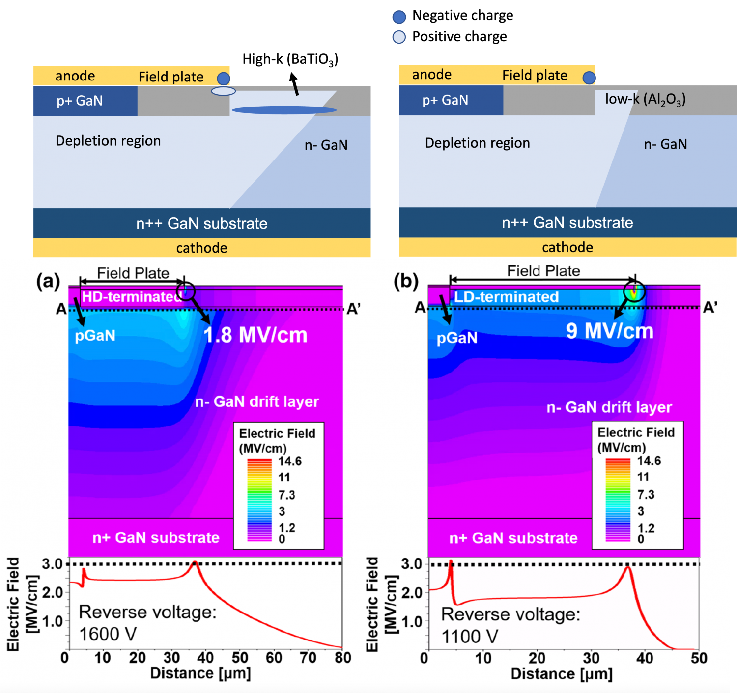
Integration of dissimilar materials for improved functionality: One significant challenge in ultra-wide band gap semiconductors is the lack of diverse functionalities within a single material system. To overcome this, we explore integration of different ultra-wide band gap material systems with each other and with other material systems. In our previous research work, an example of one such integration to improve the breakdown performance was shown through the use of perovskite oxide dielectrics (BaTiO3) on Ga2O3. These high permittivity dielectrics can enable smooth electric field profiles between the gate and drain in lateral devices, increasing the breakdown voltage. Going forward numerous such integration strategies need to be carefully studied.