
Our research direction
Our team pioneers the discovery, synthesis, and integration of next-generation materials. From atomically thin semiconductors to quantum materials, we develop and manufacture novel material systems that are industry-compatible, scalable, and highly tunable for real-world impact. We make new materials, discover new effects/functionalities, and find creative ways to bring them to public use. Our research empowers breakthroughs in electronics, sensing, defense, energy, sustainability, and environmental technologies. We leverage core principles of materials science and engineering, including microstructure, corrosion, kinetics/thermodynamics, atomic-scale deposition, materials physics, phase diagrams, and defect and dopant engineering, to guide our research and innovation.
We promise, no one is making us do this. We just genuinely love materials.
Current projects that keep us busy in our labs
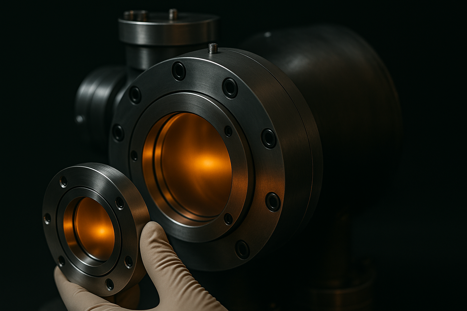
PLD deposition of High Mobility Semiconductors
In collaboration with Prof. Sanchez (ECE), we are developing new growth techniques for materials like Bi2O2Se, Sb2O2Se, Bi2SeO5, and Bi2O2Te. Starting with 1 cm² samples and expanding to 2-inch scales, we aim to create high-performance transistors using planar FET geometries.

High Pressure Materials Growth
Utilizing state-of-the-art high-pressure growth chambers, our team aims to design, engineer, and fabricate new phases of vdW and 2D materials, leading to the creation of materials previously unknown to science.

Manufacturing of MOFs for sustainability
In collaboration with Prof. Westerhoff (Sustainability), our team is addressing the scalability challenges of metal-organic frameworks (MOFs). Our goal is to develop large-scale MOFs for effective carbon capture and conversion into useful organic compounds, as well as for the removal of pollutants from water.

CHIPS Act: Manufacturing of Next-Generation Semiconductors
This project focuses on establishing advanced manufacturing tools to produce high-performance electronic materials on scales ranging from 1 cm² to 8 inches in diameter, supporting both national defense and civilian applications.

2D Janus Materials: Spintronics, Excitonics, Optics, Microscopy, and Manufacturing
Janus materials, named after the two-faced Roman god, are 2D materials with different atomic arrangements on their surfaces. This project focuses on their synthesis, understanding excitonic properties.
Discovery and Engineering of Next-Generation Metal Interconnects
As electronic devices shrink, existing copper interconnects become inefficient. This project seeks to discover new metal interconnects and develop manufacturing methods to replace copper, aiming to reduce resistivity and power consumption at scales approaching 5 nm

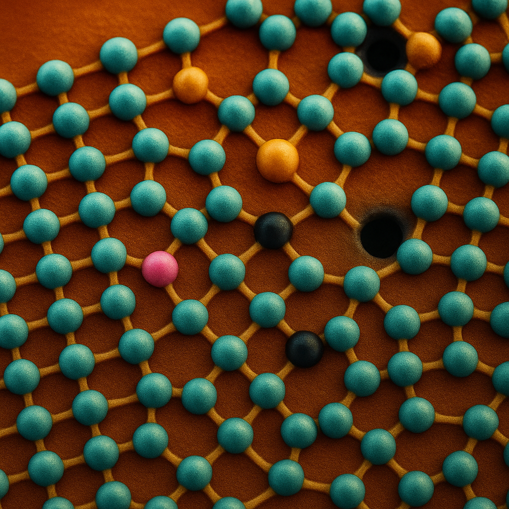
Inorganic Chiral Materials
Recently, van der Waals (vdW) inorganic chiral materials have garnered interest due to their unique structural, spintronic, chiral phononic, and quantum properties. This project focuses on discovering and realizing chiral materials, and using microscopy and spectroscopy to understand their behavior.

Materials under Extreme
We are investigating the behavior of cutting-edge material systems under extreme pressures, temperatures, irradiation, and gases. We aim to find materials ideally suited for specific applications in electronics and national security.

Atomic Microscopy and Imperfections
Advanced electron microscopy techniques are employed to study 2D Janus, 2D materials, and vdW crystals. We are investigating the nature and properties of defects, grain boundaries, and phase transitions, exploring new phases of matter.

Discovery, Engineering, and Manufacturing of 2D Magnets
Using cutting-edge microscopy and spectroscopy, we are exploring the magnetic properties of newly discovered 2D magnets. Our research aims to scale up the manufacturing of these materials for use in everyday electronics and sensing applications.
Tungsten Based Alloys
Joint initiative with Applied Materials focused on advancing tungsten and tungsten-based alloys for high-performance halogen light sources. Emphasis is placed on microstructure evolution during manufacturing and operation, as well as on advanced metrology and predictive modeling to guide material design.

Environmental Stability & Chemistry of 2D Materials
Study of degradation kinetics in environmentally sensitive halide- and telluride-containing quantum materials (e.g., 2D magnets). The project uses in-situ spectroscopy, click-chemistry, aryl salts, and carboxyl functionalization to enhance material stability while preserving or discovering new quantum properties.

Surface Chemistry & Designer Functionalization
Refinement of chemical passivation strategies through adsorption isotherm modeling and surface kinetics studies for consistent, scalable material stability solutions.
Electronic Dopants in 2D Materials
Integration of n-type and p-type dopants in TMDs, Bi2O2Se, and related 2D semiconductors to tailor electronic band structures, enhance mobility, solve electrostatics challenges of ultrascaled devices, and enable device-level performance tuning.

2D materials based IR detectors
Integration of quaternary 2D oxychalcogenides for next-generation infrared detectors and sensing platforms targeted at military and national security applications. The project aims to make materials and devices that offer tunable bandgaps, high carrier mobility, and strong photoresponse across the mid- and long-wave IR spectrum.