vdW Crystal Growth
What is a bulk crystal growth and its technological importance?
Bulk crystal growth is a process used to produce large, high-quality crystals from a small seed crystal, starting precursors, or chemical agents. Bulk crystal growth is critically important for technology as it forms the foundation for numerous high-tech applications. High-quality bulk crystals are essential for the development of semiconductors, which are the backbone of modern electronics including computers, smartphones, and solar cells. The precise and controlled growth of these crystals ensures the optimal performance of electronic devices by providing materials with minimal defects and uniform properties. Additionally, bulk crystal growth is pivotal in the production of advanced materials used in optics, such as laser components and sensors, further driving innovation in communication, medical, and defense technologies.
Our Research Directions towards Bulk Crystal Growth
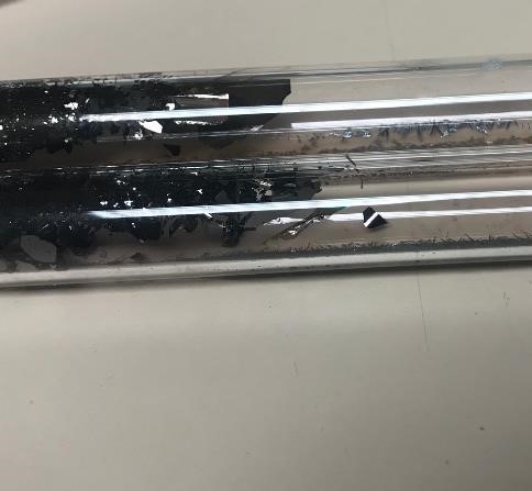
Part of our team focuses on innovative crystal growth techniques, including Bridgman growth, chemical vapor transport, hydrothermal synthesis, and high-pressure anvil cell growth, to produce crystals with 6N or higher purity and to introduce specific types and amounts of defects into the crystal matrix. Focus material systems include materials for next-gen electronics and quantum information, but special emphasis is also placed on discovering completely new materials for new advanced properties in electronics, information technologies, and sustainable energy. In particular, we focus on layered van der Waals (vdW) material systems. These synthesized crystals are characterized using advanced materials techniques to assess and engineer their properties. Some examples include, but not limited to, quantum transport measurements, optical spectroscopy, and scanning transmission electron microscopy to resolve sub-Angstrom details of our lab-grown materials, allowing us to directly visualize various defects (vacancies, adatoms, grain boundaries, etc.), which is essential for understanding the atomic-scale effects of defect engineering on intrinsic host materials.
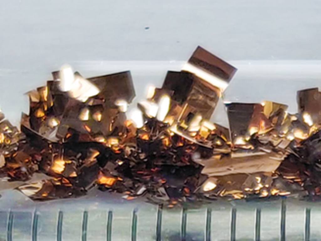
Some of the example focus crystal systems include;
- 2D high mobility semiconductors: Bi2O2Se and Bi2O2Te
- 2D magnets such as MnPS3, Fe2GeTe3, CrOCl, CrI3, NiI2, FeI3, TiBr3, and many others
- 2D excitonic semiconductors: MoSe2, WSe2, WS2, and WTe2
- 2D anisotropic materials: TiS3, ReS2, MoTe2, Tellurene, ZrSe3, and HfTe5
- Chiral materials: SnPI and InSeI
- Other quantum crystals: GdTe3, LaTe2, HfTe3, ZrTeP, and ZrSiSe
Fundamental Research Questions
- What are the kinetics and thermodynamics of reaction to enable the synthesis of new bulk crystals?
- What are the governing rules for engineering crystal quality (defect density, single crystal domain size, etc.)?
- What new phases of materials can be synthesized using high pressure anvil growth chambers at high pressures (>40GPa)
- What are the fundamental growth parameters to synthesize bulk crystals are large scales
Publications and Patents: Our team publishes Nature, Science, and other high impact journal each and every year and these publications heavily rely on our ability produce new and highest quality crystals. Our team also holds a large number of U.S patents and patent applications on these novel crystal growth techniques.Types of Quantum Crystal