Research
Our research focuses on developing novel electronic design automation (EDA) tools and computer-aided design techniques for VLSI systems. Our current interests include the following:
1) Machine learning for EDA and open-source EDA
a) ML EDA Research
The semiconductor industry faces several challenges with traditional Electronic Design Automation (EDA) tools, including limited scalability, high complexity, and reliance on heuristic-based approaches that often sacrifice accuracy for speed. At ASU-VDA Lab, we’re addressing these issues by leveraging cutting-edge Artificial Intelligence (AI) and Machine Learning (ML) techniques.
Challenges with Traditional EDA Tools
- Heuristic-Based Approaches: These methods tend to prioritize speed over accuracy, leading to suboptimal design solutions.
- High Barrier to Entry: Traditional tools can be difficult for non-experts to use effectively, limiting their accessibility.
- Limited Scalability: With polynomial time complexity, traditional tools struggle to scale with new technologies and large systems, such as those containing trillions of transistors.
AI-Driven Solutions for Automation and Optimization
To overcome these barriers, ASU-VDA Lab is exploring innovative AI-driven approaches to enhance both automation and optimization in EDA processes.
Leveraging Large Language Models (LLMs) for Automation
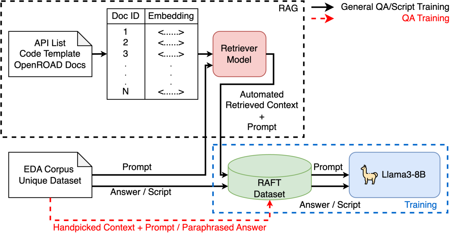
To lower entry barriers and streamline the automation of EDA tasks, we are developing chatbots and specialized datasets for ML-driven EDA script generation. A key example is the OpenROAD Assistant, which fine-tunes the LLaMA2 model to answer questions related to the open-source EDA tool, OpenROAD, and generate scripts to perform physical design tasks, as shown in the figure on the right. To further enhance these models, ASU-VDA is building specialized datasets, including the EDA Corpus for LLMs, BeGAN for layout related data generation and synthetic netlists.
AI-Powered Fast Analysis for EDA
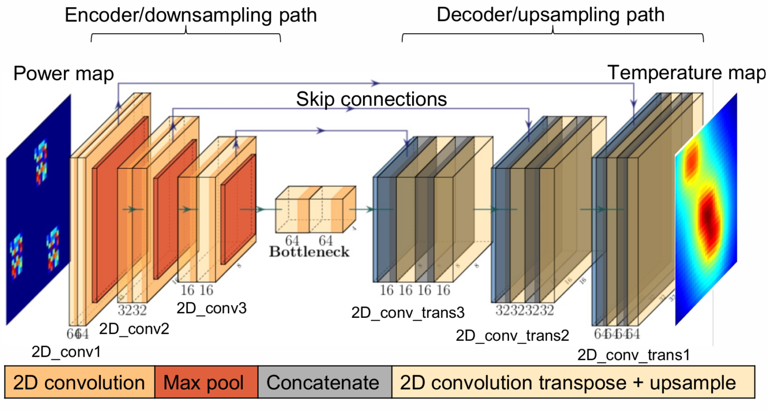
In addition to improving automation, fast and accurate analysis remains a critical challenge in EDA. As part of our research, we’ve developed AI models for inrush current analysis, IR drop analysis, and thermal behavior analysis. These models utilize image-based AI techniques to enable rapid performance insights, significantly improving design efficiency and reducing time-to-market.
Graph Neural Networks (GNN) for Netlist Optimization
Another exciting area of our research focuses on using Graph Neural Networks (GNNs) for optimizing netlists, particularly for tasks such as gate sizing and buffer insertion. GNNs offer the potential to model and optimize complex circuit structures more efficiently, improving performance and reducing the time needed to design optimized systems.

b) ML EDA Infrastructure
ML for EDA is a growing research area, but it lacks infrastructure. ASU-VDA has developed infrastructure using OpenROAD to provide a playground for EDA researchers. This infrastructure has three key pieces:
- Python APIs to EDA tools: OpenROAD provides interfaces that wrap underlying EDA tool C++ APIs, ensuring faster data generation than commercial tools’ slower TCL interfaces.
- ML-Ready Data Formats: NVIDIA has recently proposed CircuitOps in collaboration with ASU-VDA lab, an ML-friendly data format that leverages OpenROAD to model chip data as labeled property graphs, utilizing pandas data frames to store graph properties as features. This combination, together with OpenROAD’s Python APIs, streamlines the integration of ML algorithms into the EDA tool infrastructure.
- ML inference and callbacks to the EDA world: OpenROAD is developing Python APIs to facilitate the integration of ML inference results into its database, establishing a feedback loop between ML algorithms and EDA tools.
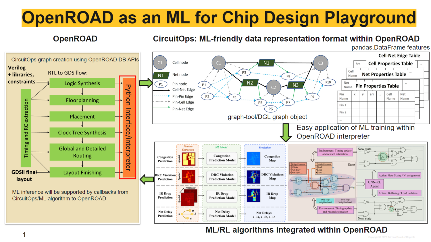
This infrastructure, depicted above, can be a launchpad for developing ML-powered chip design optimization algorithms. We have a tutorial on utilizing this infrastructure.
2) Design for sustainable computing
All aspects of computing, from small chips to large datacenters, come with a carbon footprint (CFP) price tag. For several decades, the semiconductor industry has focused on making chips smaller, faster, and less power-hungry, but few efforts have considered the impact on the environment. The dramatic increase in the demand for compute in the past two decades, fueled by new applications (e.g., artificial intelligence) that demand at-edge and at-cloud-scale computing, has resulted in the information and computing technology (ICT) sector, contributing to more than 2% of the world’s CFP – half that of the aviation industry and projected to surpass it in the next decade if left unchecked
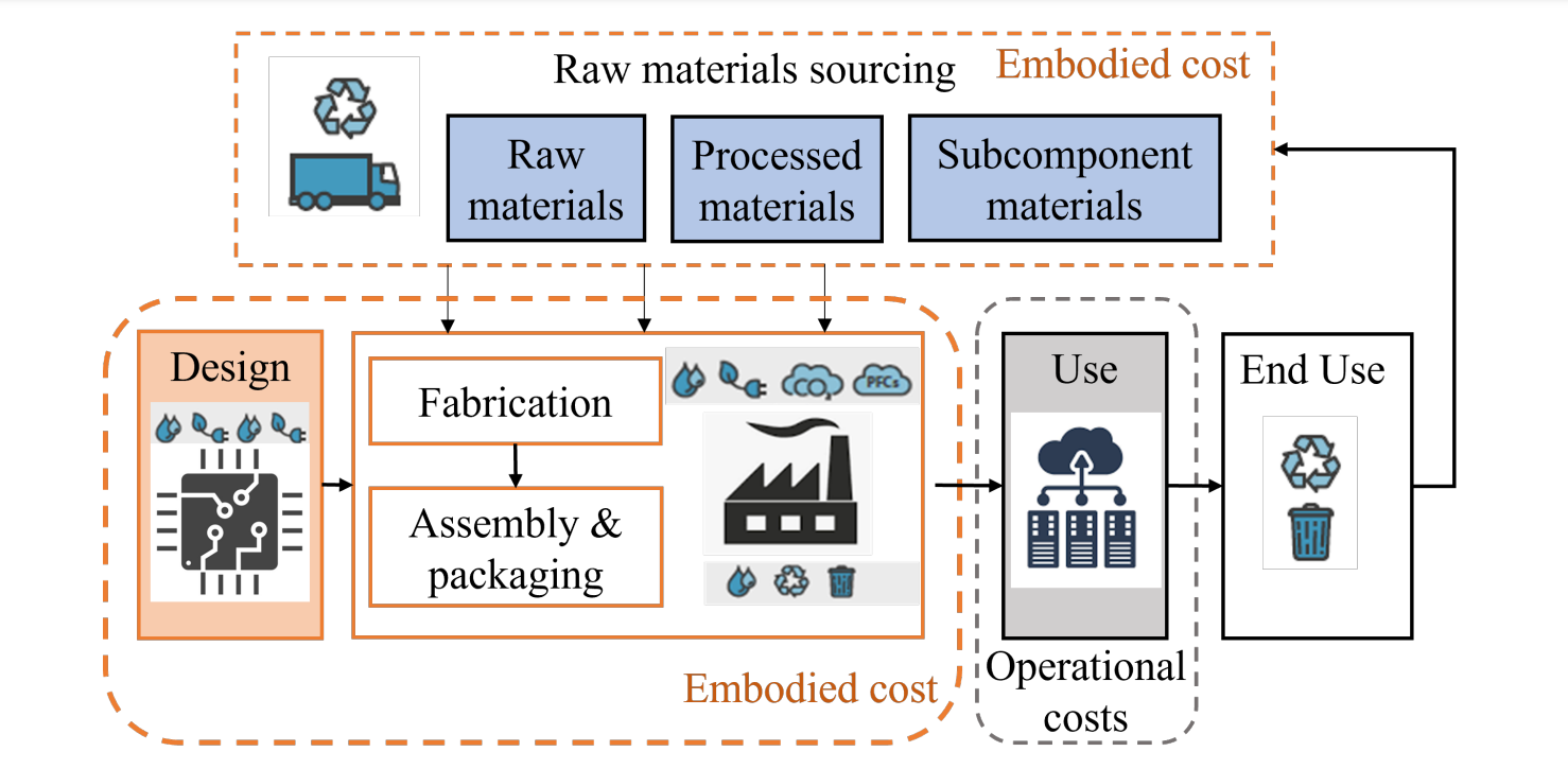
The figure above shows the life cycle assessment (LCA) of a semiconductor product and highlights the different sources of
greenhouse gases (GHG) in the life of product. The operational costs refer to the CFP generated by the end user, which, in the case of a data center, are the data-to-day activities that draw energy. The embodied costs are the costs that come from the design, manufacturing, packaging, and materials sourcing of the server class computation resources in the data center. While technology scaling and electronic design automation have helped to design energy-efficient VLSI systems with lower operational CFP, the environmental footprint has continued to increase over the past decade and is now dominated by carbon emissions from chip design and manufacturing, i.e., the embodied CFP, especially for low-power edge devices. It is imperative to look beyond the metrics of low power and energy efficiency and include total CFP (embodied and operational) as a first-order optimization metric for the sustainable use of today’s modern computing devices. Several technology companies have pledged to limit their CFP, which can only be achieved by adopting approaches that are cognizant of CFP.
VDA Lab aims to develop algorithms and frameworks for the design of sustainable computing across the entire technology stack from algorithms to devices. We have approached the design of sustainable systems via the use of heterogeneous integration, and reconfigurability thus far.