Our facilities
Our lab is dedicated to cutting-edge materials manufacturing, processing, and metrology, offering students and researchers unparalleled hands-on experience with some of the most advanced tools in the world. We emphasize top-tier training on state-of-the-art equipment, preparing the next generation of scientists and engineers for careers in academia, industry, and beyond.
Materials synthesis and manufacturing
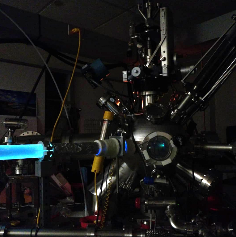
We offer a comprehensive suite of thin film and bulk crystal growth techniques for both research and training purposes. Our thin film systems include MBE, multiple CVDsPECVD, PLD, and sputtering. For bulk growth, we utilize CVT, Bridgman growth, hydrothermal synthesis, and high-pressure anvil growth systems.
Metrology and characterization
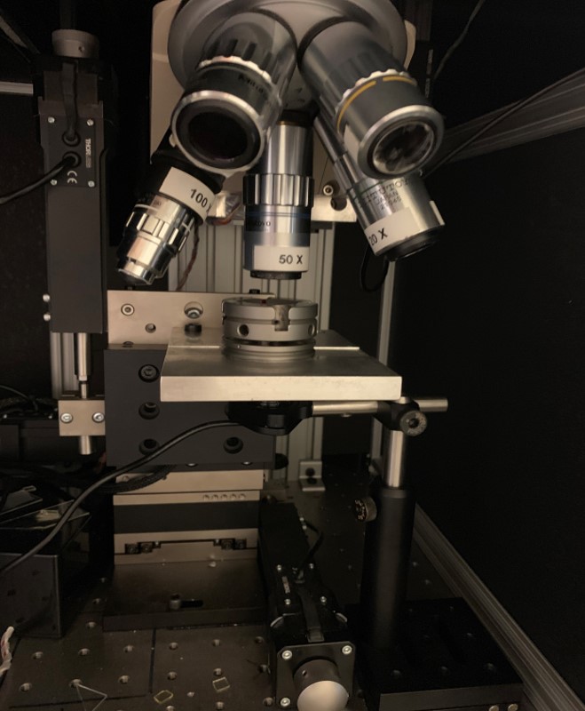
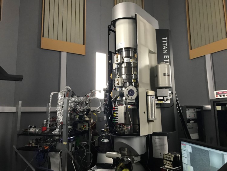
Our team specializes in precision characterization of nanoscale materials using a wide array of advanced tools. These include AFM, STM/STS, TEM/STEM, and various optical spectroscopy techniques. Measurements span extreme conditions (from cryogenic temperatures (~1.7K) to elevated thermal regimes (~1400 K). The lab is also equipped with PPMS, VSM, MPMS, nanoindentation platforms, and AFM nanoindenter systems for probing electronic, magnetic, and mechanical properties. Catalysis stations and nano-catalysis AFM/STM systems enable exploration of electrochemical and artificial photosynthesis phenomena under controlled gas, liquid, and vacuum environments.
Processing and application
We support an extensive range of materials processing techniques that bridge the gap between fundamental synthesis and real-world applications. We further transition these materials into functional applications through cleanroom-based device fabrication, prototyping, and system-level integration
Tour of our facilities


🔬 Core Units & Capabilities
– Thin Film Deposition: MBE, CVD, PECVD, PLD, sputter
– Bulk Crystal Growth: CVT, Bridgman, Hydrothermal, High-Pressure
– Advanced metrology: AFM, STM/STS, TEM/STEM, PPMS, MPMS, VSM, Optical spectroscopy, electronic transport, XRD, XPS, WDS, EDS, SAXS, and FTIR
– Material Processing: Plasma Chambers, Vacuum Furnaces, Exfoliation Benches, fumehoods, glovebox stations, and mechanical testers
– Fabrication: Cleanroom Access Lithography, Metallization, Packaging, Functional Device Fabrication (FETs, Memristors, Sensors)
Join us in Shaping the Future
Interested in collaboration, research opportunities, educational outreach, or learning more about our innovations? Whether you’re a student, partner, or member of the public, we invite you to be part of our journey.