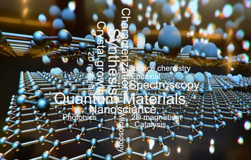
The research within our team is involved in cutting-edge initiatives aimed at manufacturing next-generation materials tailored for electronics applications and sustainability solutions. Leveraging advanced materials manufacturing techniques, our team focuses on developing innovative approaches to create materials with enhanced properties and functionalities. Our efforts extend to sustainability challenges, including the removal of pollutants from water and the valorization of carbon through novel material systems. Through innovative bulk crystal growth and high-pressure synthesis methods, we aim to discover new material systems with unprecedented characteristics and applications. Furthermore, our research endeavors are complemented by in-depth investigations into material behavior and performance using a range of sophisticated techniques, including microscopy, spectroscopy, and electronic measurements. By combining expertise across various disciplines, we strive to drive forward the frontiers of materials science and engineering, addressing critical societal needs and advancing technological innovation.
Funding. Recognizing our creating work, our team is supported by DARPA CHIPS act, Army Research Office, the Department of Energy, National Science Foundation, Arizona Water Initiative, Intel, Applied Materials, Lawrence Semiconductors, and other agencies.
Reputation. Our team is one of the leaders in materials discoveries in the world. Our team has been recognized both domestically and internationally with prestigious awards including Highly Cited Researcher awards in 2019, 2020, 2021, 2022, and 2023, PECASE award by the President Trump, the Ten Outstanding Young Person award, Jewish National Funds Awards, and many others. Recognized Top 10 in the world by citations (Google Scholar). Our research team is funded by the federal government agencies such as the National Science Foundation (NSF), Department of Energy (DOE), Army Research Office (ARO), CHIPS act, Arizona Water Initiative as well as industries such as Lawrence Semiconductors, Applied Materials, and others.
Student training. Our research directions and existing facilities allow our undergraduate, master’s and Ph.D students as well as postdoctoral researchers to get hands on experience on variety of sophisticated tools that are highly desired in industry and academia. Some examples include Materials synthesis (CVD, PLD, MBE, PECVD, ALD, MOCVD, crystal growth), characterization (TEM, AFM, SEM, EDS, optical microscopy, spectroscopy), and many others. By the completion of their terminal degrees and their projects, our alumni smoothly transition to academe or industry.
So far, our work has made a broad impact in applied and fundamental sciences and has been widely covered by the popular media sources such as Scientific American, Nature Publications, MIT news, Institute of Physics, Phys.Org, Technology, Gizmag and various other news outlets.
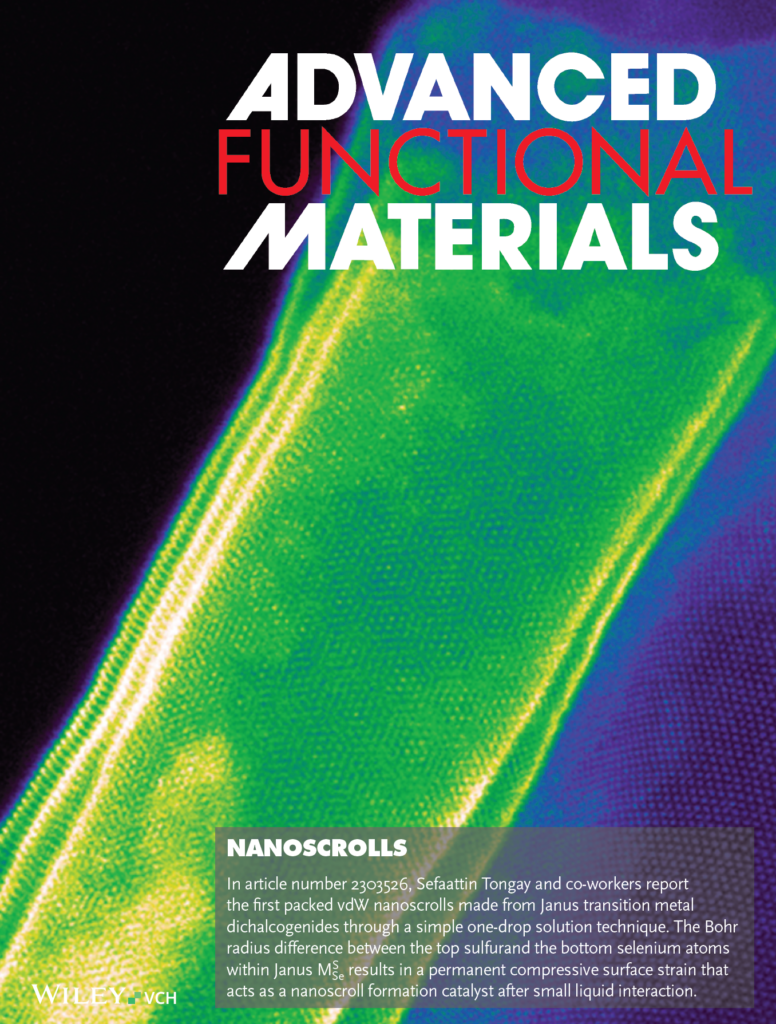
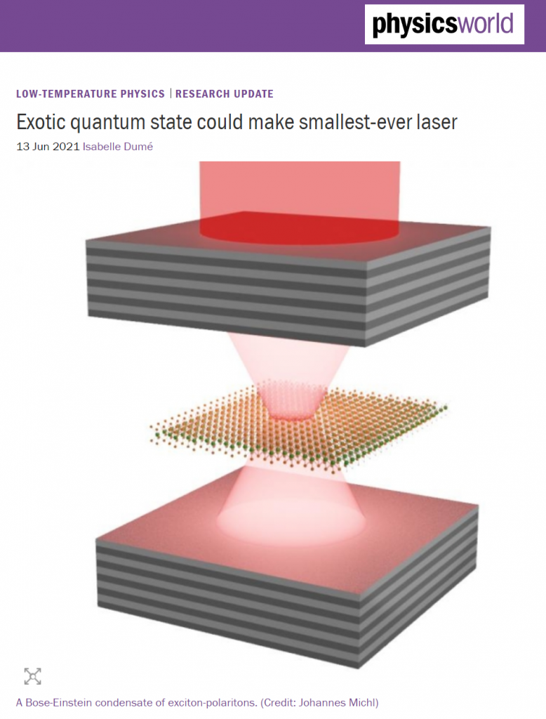
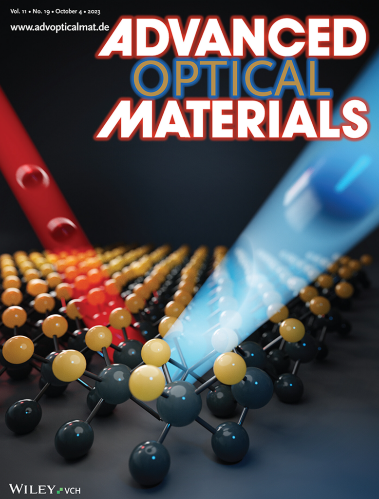
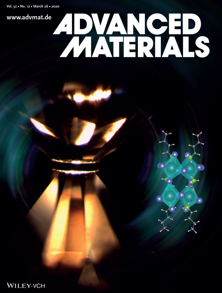
Some of the Magazine Cover Images Highlighting our Research