

Our research cluster team has been awarded a substantial $250 million grant from the U.S. government under the CHIPS and Science Act to be one of the HUB partners to commercialize next-generation semiconductors at large scales. This funding will propel our groundbreaking work in developing next-generation material systems that hold the promise of revolutionizing various industries, from electronics to quantum communications technologies.
Focus Areas
1. Advanced Electronics Manufacturing
Our primary focus is on creating advanced material systems that will drive the next generation of electronics. Leveraging cutting-edge manufacturing techniques, we aim to develop materials that enhance the performance, efficiency, and scalability of electronic devices. Example material systems include WSe2, Bi2O2Se, graphene, and other layered 2D materials
2. Quantum Communications
In the realm of quantum communications, we are exploring new materials that can support the secure and efficient transmission of information. Our work aims to lay the foundation for the next leap in communication technology, which promises unparalleled security and speed.
Innovative Techniques and Approaches
Our team employs an array of state-of-the-art materials synthesis, deposition, and manufacturing techniques to create and refine these advanced materials:
- Discovery, Design, and Engineering of New Deposition Systems
- Atomic Layer Deposition (ALD)
- Pulsed Laser Deposition (PLD)
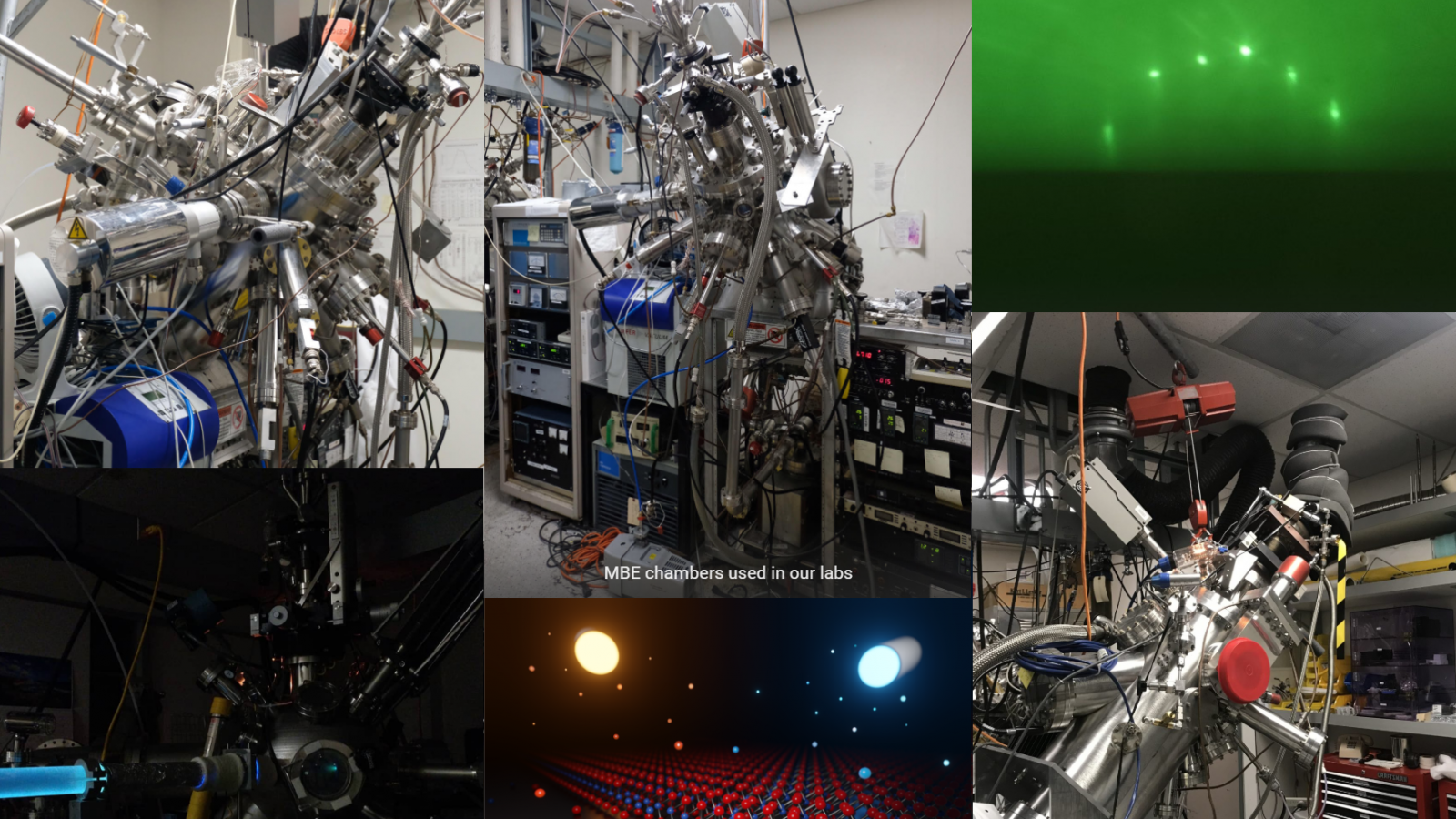
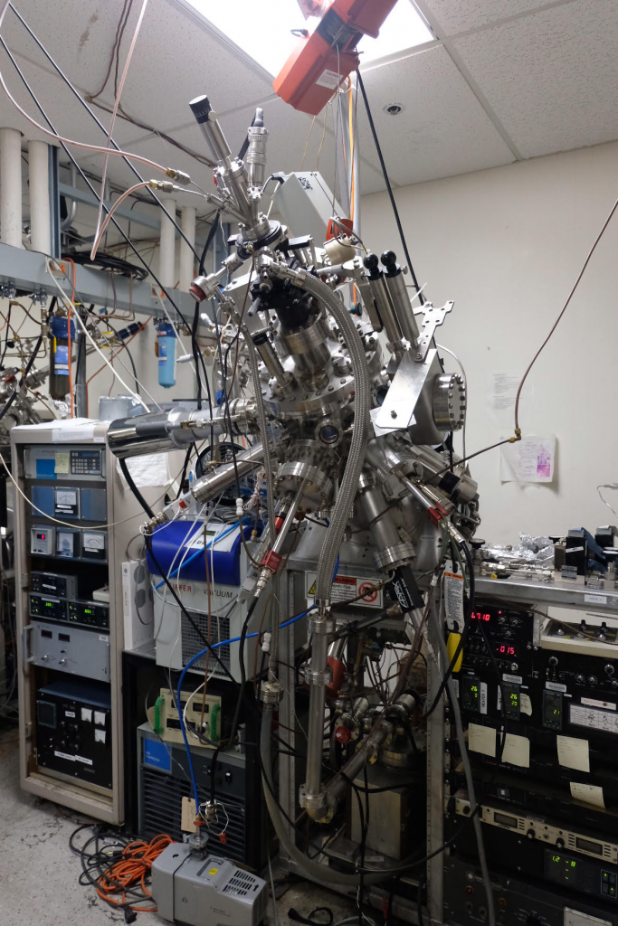
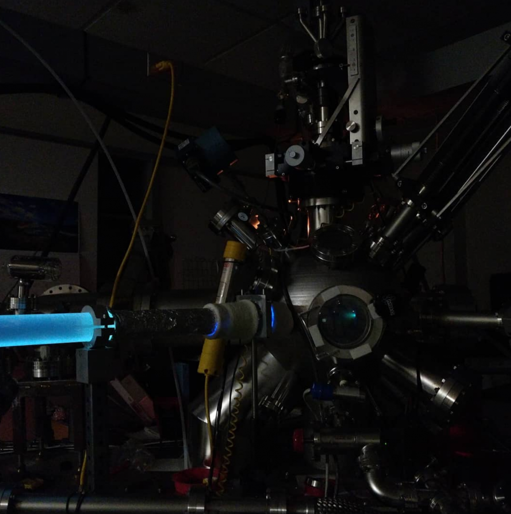
- Molecular Beam Epitaxy (MBE)
- Metal-Organic Chemical Vapor Deposition (MOCVD)
- Plasma-Enhanced Chemical Vapor Deposition (PECVD)
These techniques allow us to manufacture research-grade materials at large scales, paving the way for their transition from the lab to real-world applications.
Fundamental Research Questions
- What are the thermodynamics and kinetics of reactions that enable the 2 to 8-inch wafer-scale synthesis of 2D materials?
- What are the governing rules for introducing electronically active point defects to create functional materials in electronics?
- What are the fundamental mechanisms for achieving control over point and grain boundary defects to reach ultimate material perfection?
- What are the possible chemical reactions that enable the manufacturing of these materials at CMOS-compatible temperatures?
- What are the fundamental processes for manufacturing these next-gen materials in parallel with existing CMOS processes?
Impact and Applications
The materials developed through this initiative will have wide-ranging applications, including:
- National Defense: Enhancing the capabilities and resilience of defense technologies.
- Civilian Use: Improving consumer electronics, environmental sustainability solutions, and communication infrastructure.
Our team is excited to lead this ambitious project, which not only represents a significant milestone for our institution but also holds the potential to make a profound impact on society. We are grateful for the support provided by the CHIPS Act and look forward to sharing our progress and innovations with the broader community.

Select publications
Our team has produced a large number of Nature, science, and other high impact journals on these topics over the years and since 2014 at Arizona State University. Full list can be access at Google Scholar profile.